Close
0%
0%

LCPU - A CPU in LED-Transistor-Logic (LTL)

This projects tracks my efforts to develop discrete LED-Transistor logic building blocks and designing a CPU from them.

timTim
Similar projects worth following

Many years ago I completed the challenge to fit a CPU into the smallest available CPLD on the market - the MCPU. Ever since then I have been pondering about a new challenge in minimalism in CPU-Design. I had completed a TTL-based CPU even before the MCPU. Clearly, the only direction left is to go fully discrete and build a minimal CPU out of discrete transistors. 

To make things interesting and add a modern twist, I decided to investigate a logic family that uses light emitting diodes (LEDs) as an active element. LTL is a logic family from a past that never happened. It combines 1950s transistor logic with low current green InGaN LEDs that were invented in the 1990s.

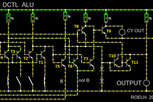
I already completed the design up to a prototype of a sub-system (see header image) and will use this project to document the steps I have taken to get there.

Start with the first log by using this link or use this link to view all project logs on one page.


  • Testing the Control Unit

    Tim05/31/2020 at 22:43 2 comments

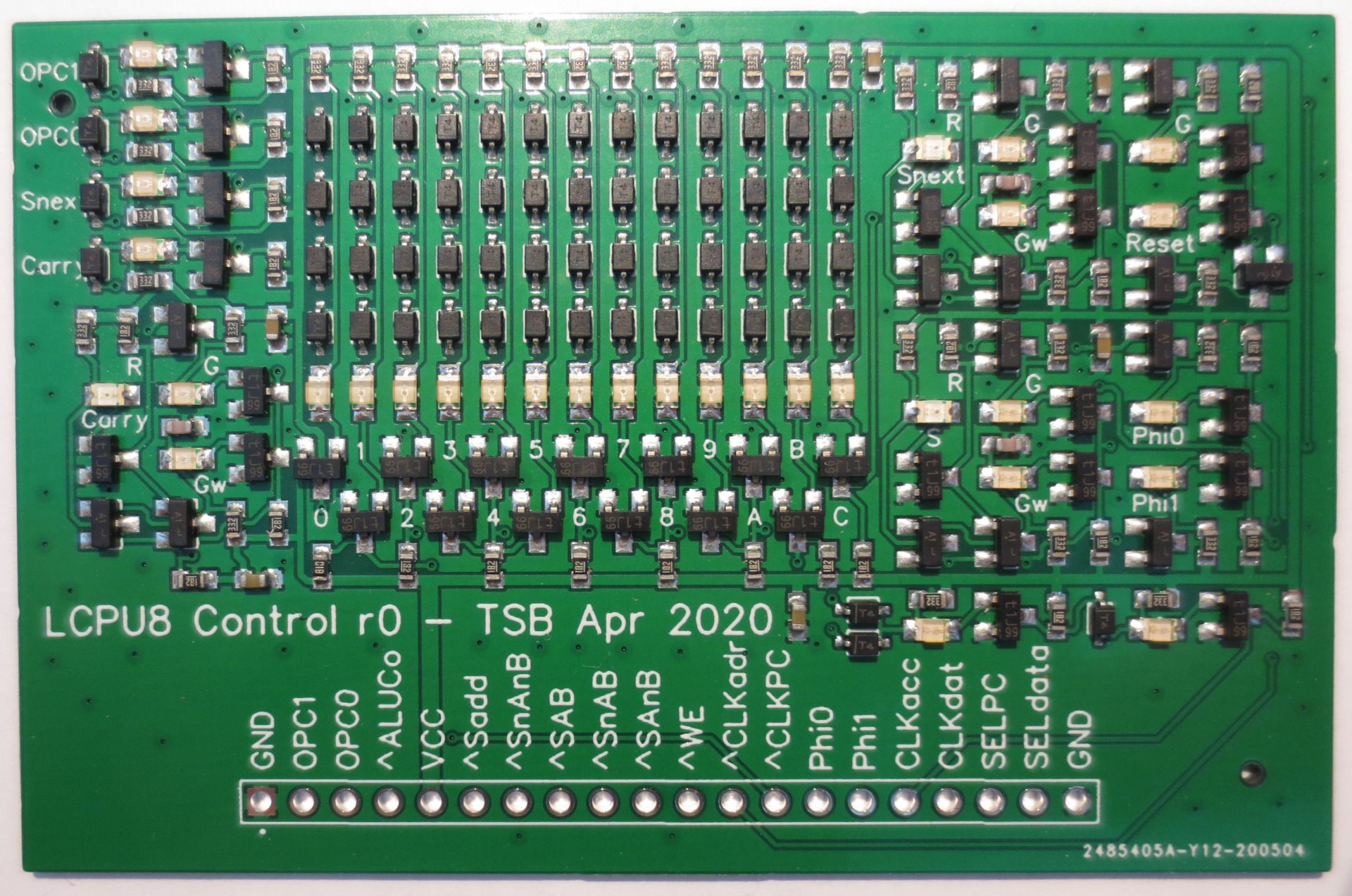
    The assembled control unit already arrived a while ago, but I only got around testing it today.

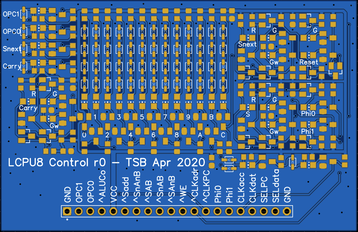
    You can see a photograph of the PCB above. Unfortunately I already noticed a stupid mistake at this level: I forgot to route the reset signal to the I/O header. Since this was a circuit level mistake, no DRC caught this. Well, luckily that's easily fixed with an additional wire directly to the reset-driver.
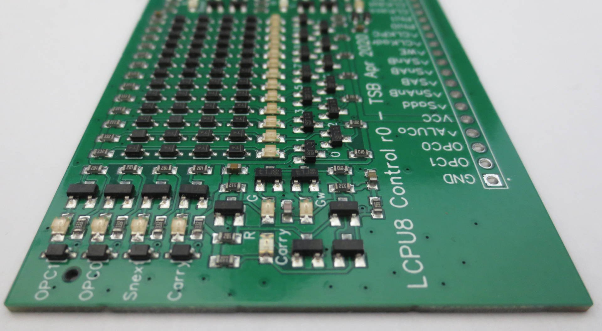
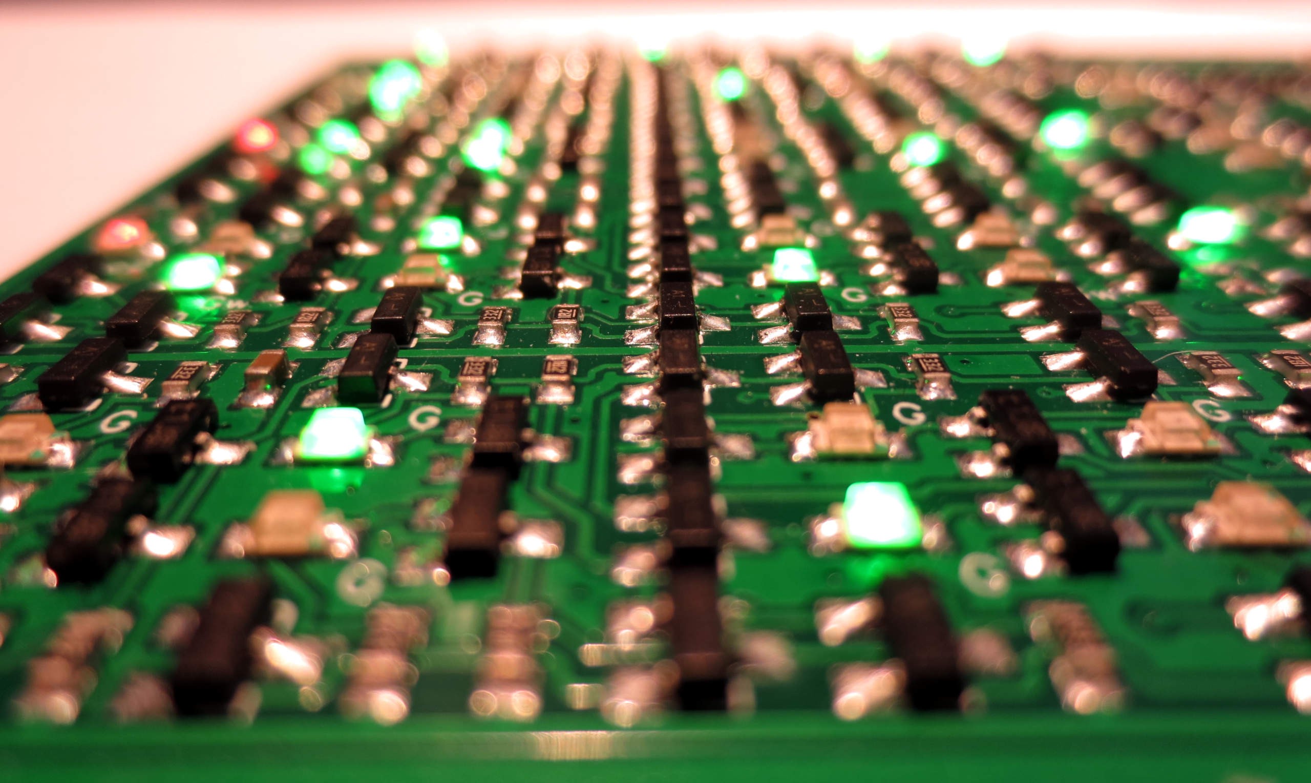
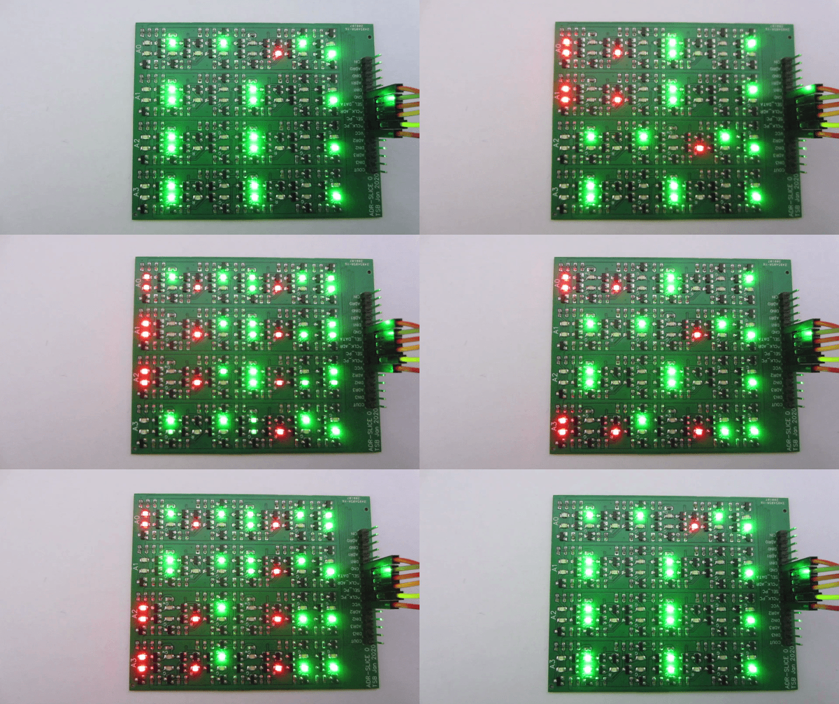
    Due to the construction of the logic array, there is a LED for every row (input) and column (minterm/output), creating a very nice regular structure. Every mintern has an output inverter and uses wired-AND as a combiner. See previous log on control unit design.
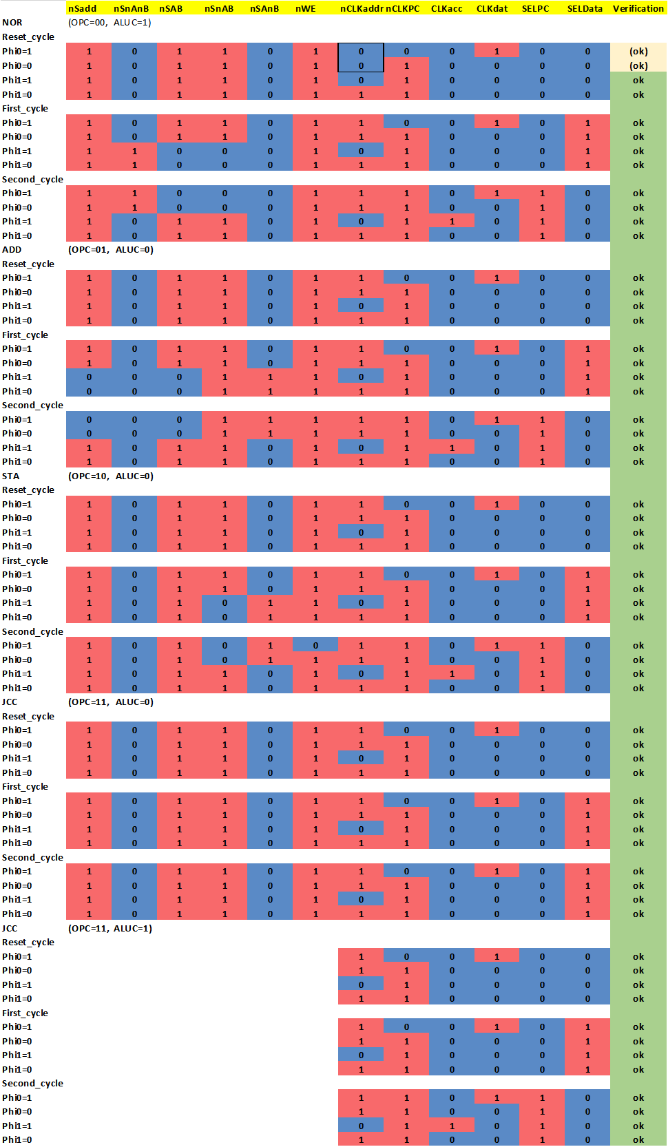
    Verifying the control unit is not that easy due to the high number of outputs with irregular behavior in combination with several internal states. I used an ATMega168 microcontroller to exercise every possible sequence and record the outputs.

    Each of the four instructions is tested individually, once for carry high and once for carry low. The state of the carry flag only plays a role for the branch instruction. Each instruction test sequence consists of three cycles: In the first cycle reset is high to reset the state registers, then the instruction is clocked for two cycles to exercise both possible instruction states. (I also tested longer sequences to make sure the state machine jumps back to S0)

    The full sequences are listed below. The output was verified in the true-and-tested "visual inspection of output waveforms" method, that is still completely ok for designs of this size.

    There is a slight misbehvaior of nCLKaddr during the first test sequence, but this is inconsequential and seems to be related to an issue with the test setup. Apart from that, everything was tested to work fine.


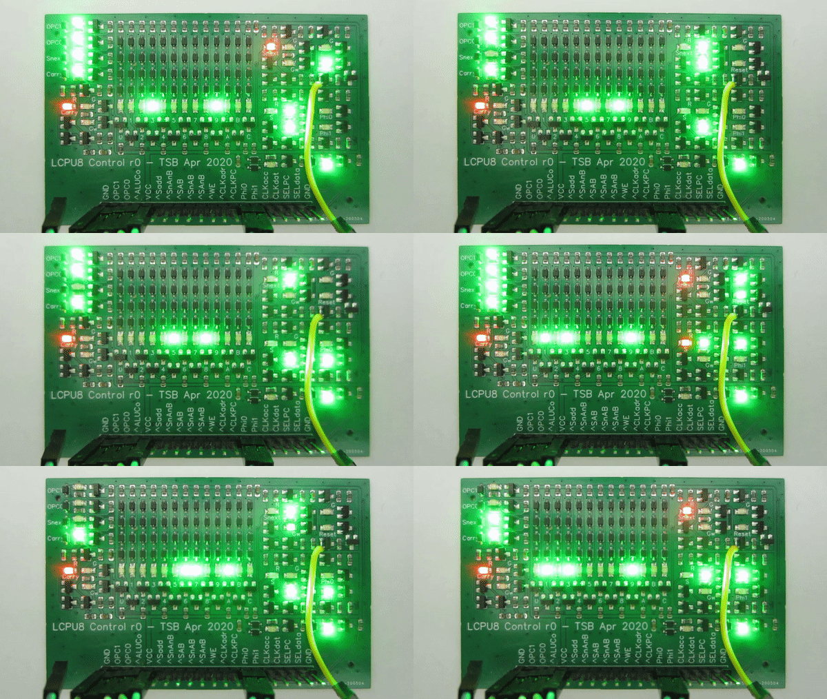
    You can see the control unit in action above. Due to it's irregular pattern, this truely seems to be "peak blinkenlight".
    The test of the control unit concludes the design of all major functional units of the LCPU: ALU, Adress path and control unit.

    Now on to a slightly more annoying part: Designing the backplane board. I still have no idea how to do it in a way that does not obscure all the nice LEDs. Apart from that, the backplane needs to hold the memory and I need to find a way to integrate bootloading and output in an efficient manner.

  • Designing the Control Unit

    Tim04/27/2020 at 20:30 0 comments

    Designing the control unit is one of the more complex tasks in MCU design. What used to be a few lines of VHDL turns out to be a tedious task when boiling it down to discrete gates. Or maybe I need a better design flow...

    Lets look at the problem at hand. The final LCPU will consist of an 8 Bit datapath and an 8 Bit adresspath. The upper two bits of the addresspath will be used for the opcode. Since both the data and the ALU board are 4 bits wide, two of each ports have to be used.

    To complete the CPU, we need a control unit that outpus the right control signals in depends of opcode and state machine cycle.

    The original MCPU has a rather simple control unit that consists of a state machine that is directly mapped to opcodes. Decoding of the states is localized at the datapath. Since the LCPU uses a bitslice approach, it is more efficient to also include decoding of states into control signal in a centralized control unit. Generally, that is a design choice that allows for extending of the design and easier bugfixing. In terms of robustness it would be better to do localized state decoding to reduce the number of control signals.

    There are 8 ALU board control inputs (Carry In, CLK_ACCU, CLK_DAT, Aluctrl[4:0]) and one output (Carry Out). The address board has 4 control inputs (SEL_PC, SEL_DATA, nCLK_PC, nCLK_ADR) and two outputs (OPC1,OPC0 -> A[7:6].

    The control board itself has a few internal registes for carry and states and inputs for a two phase clock (phi1,phi2) and reset.

    As a first step, I mapped all control signals to states and clock sub-cycles. The LCPU is still able to execute every instruction in a maximum of two clockcycles, despite switching from edge-triggered FF to latches.

    ALU control signal encoding in dependence of Opcode and state.

    Many of the simpler control signal encodings could be directly mapped to single gates. In additional you can find three latches for Carry signal and state enconding here, in what could best be described as "sea of gates". Very tedious to layout on the PCB, but straightforward in implementation by using the building blocks I designed earlier.
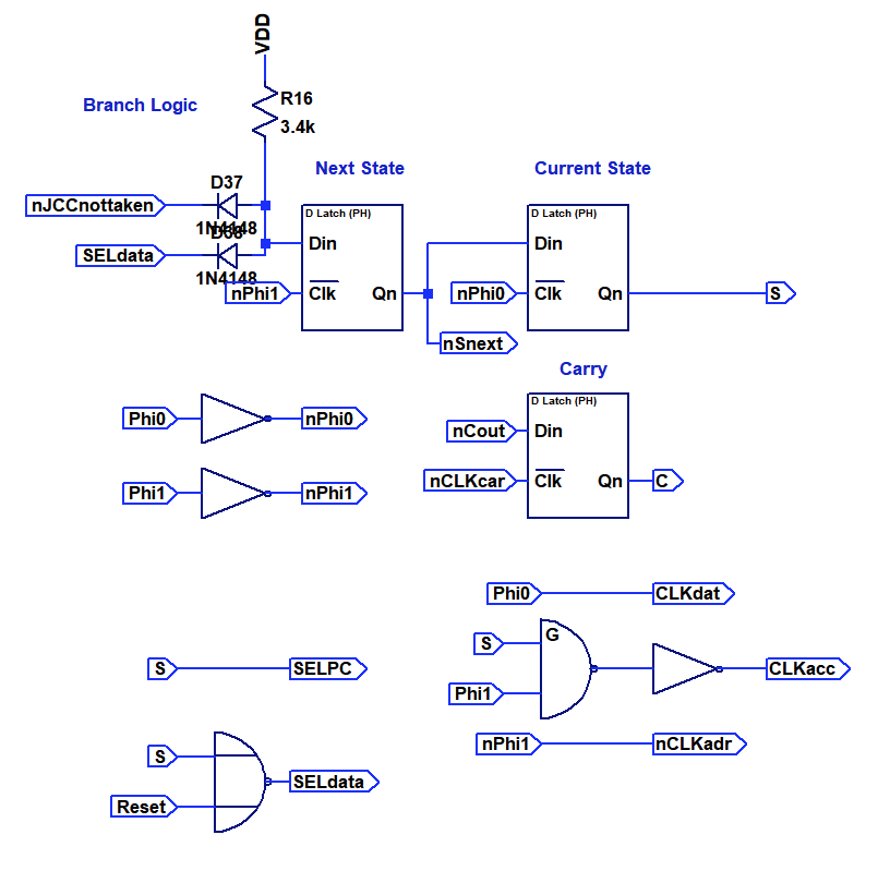
    Of much more interest is the AND-OR-INVERT logic array that is used to decode the more complex signals, specifically the opcode into ALU control signals. You can see the circuit below.
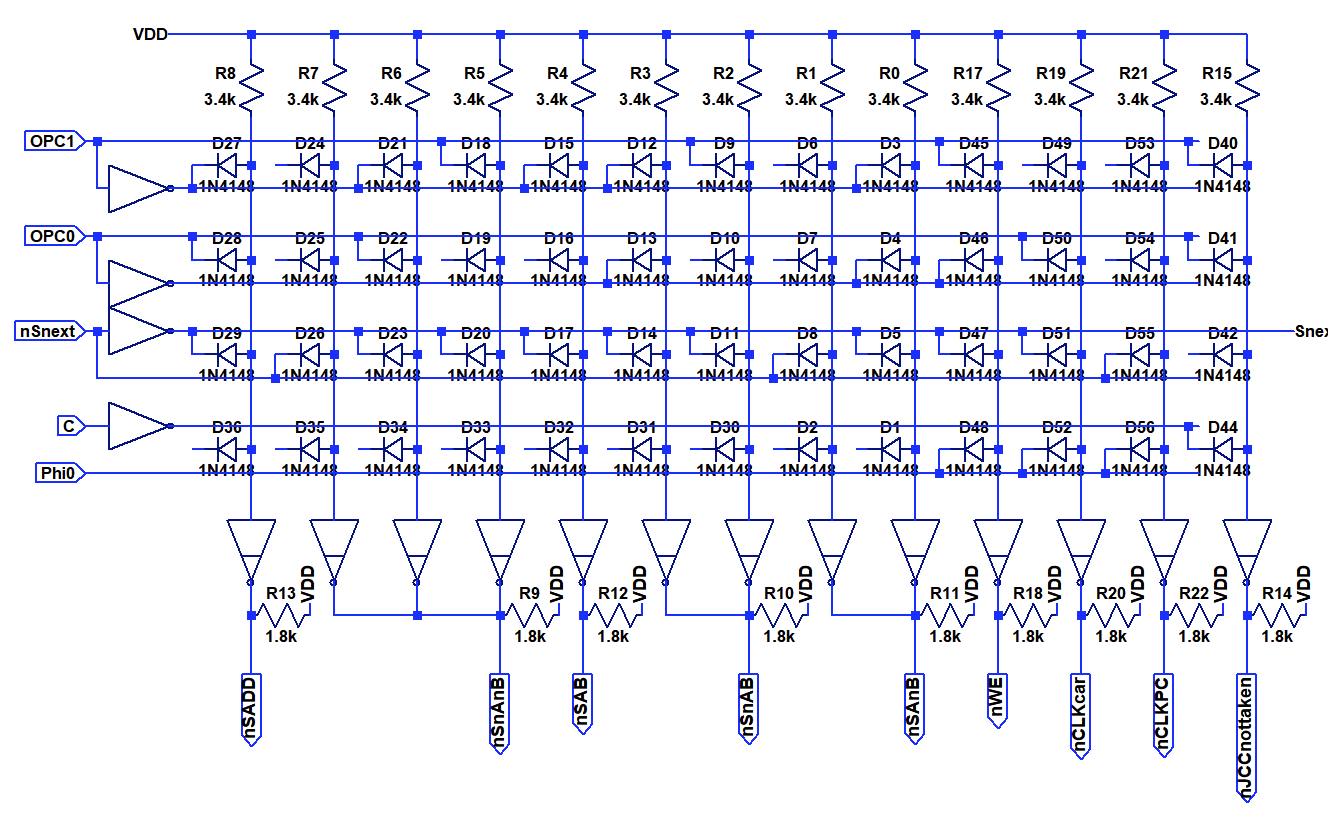
    Instead of using double diodes I switched to single diodes to allow layout in a regular matrix. Input signals are routed vertically on the rear side,  output terms vertically on the front side. Typically both the inverted and non-inverted inputs signals are provided by means of the inverters on the left side. Each column represents a multiple input AND-gate (Minterm). By connecting the diodes not at all or to the positive or negative input signal it is possible to crate any convolution of AND-operation. The opon collecter inverters at the bottom perform a "NOR" operation on any number of input terms. By combining these, it is possible to implement any boolean operation with only minimal changes in the layout. I decided to populate also unused diodes in the matrix to allow for later fixability.
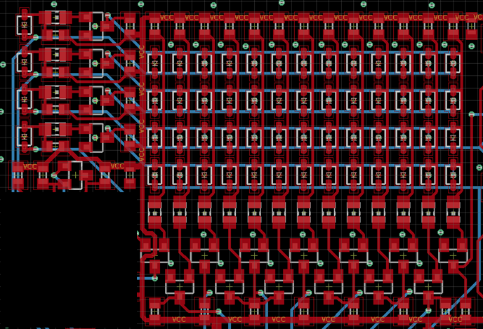
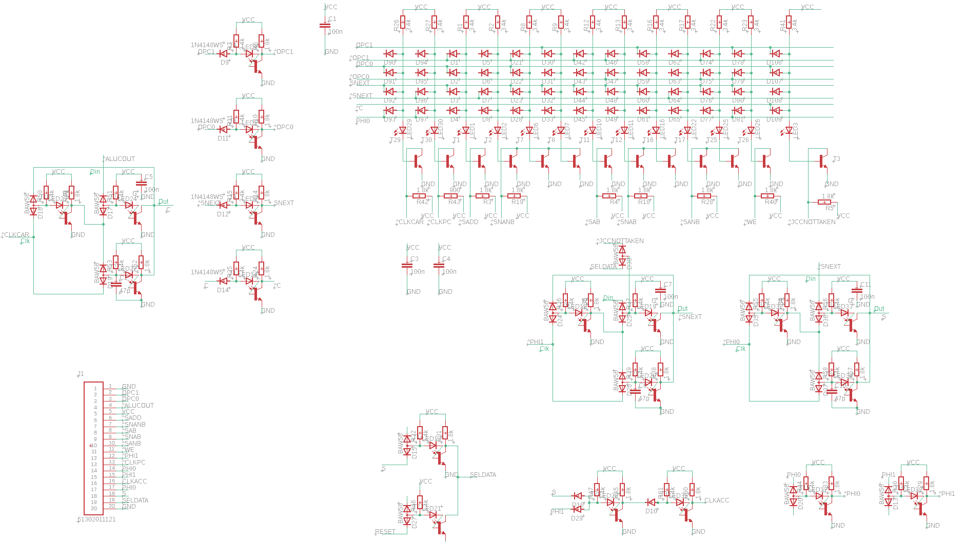
    The full layout of the logic array is shown above. As you can see, the schematic represents the arrangement of the layout quite well. The density is quite good, the full layout is just 45x33mm². Even though the array itself does not use LEDs, the input and output inverters are true LTL gates, so that blinkyness is garuanteed!
     
    For the sake of completness, the full schematics for the board level implementation are shown above.
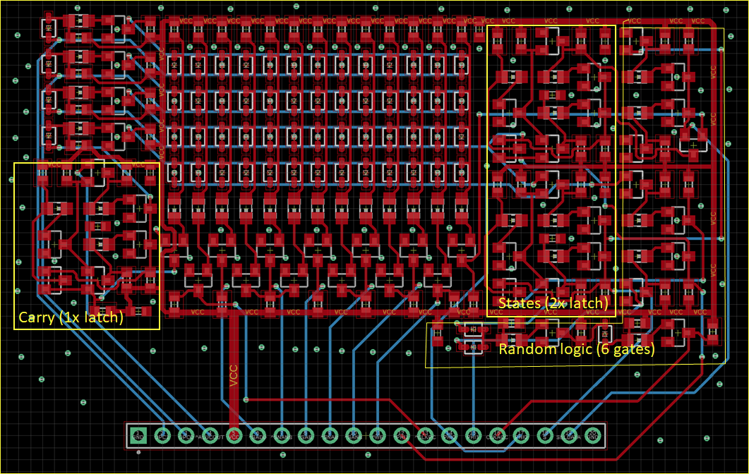
    You can see the full board with a few annotations above. (This feels like annotating an IC...). Total size is 78x50mm². Off to manufacturing...

  • Testing the ALU Board

    Tim03/28/2020 at 17:53 1 comment

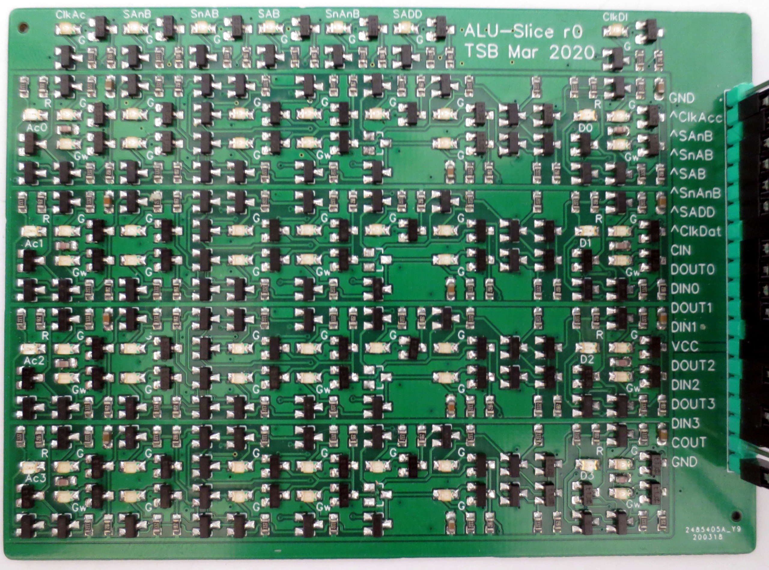
    Thanks to express shipping, the populated PCBs arrived less then a week after ordering them. A top down photo of one ALU board with 4 bitslices is shown below.
    The dual-input diodes for the boolean unit multiplexer line up neatly in one row.
    I tested the board using an ATMega168 to generate stimulus signals. Unfortunately, I found a small mistake I made earlier in the design: The generate term in the carry chain should not have an additional carry input, see below. Luckily it was easily possible to fix this by removing one diode per slice from the board. You can see the unpopulated pads in the center of the top down image.
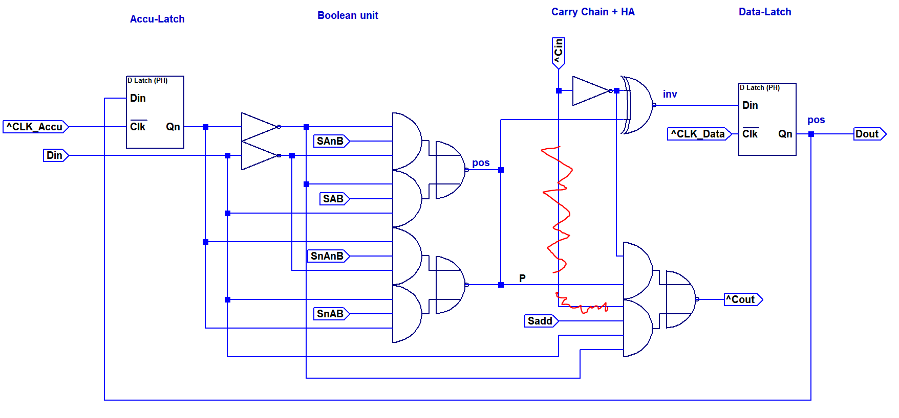
    Removing this signal would have allowed to densify the layout significantly and also add the carry-chain inverter to the output, so the carry signal is non-inverting. But well, next time...

    The list below shows the control signal configurations that were tested. Only the first three cases apply to operations that are used by the MCPU ISA. In addition, Y=B is needed for address loading.
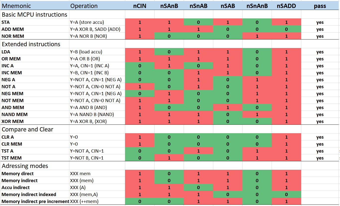
    The other operations would allow for a later extension of the instruction set.

    Clockspeed was tested up to 2 MHz. Even for the worst case (ADD with carry in=1), the signal integrity looked excellent, suggesting that also 4 MHz and higher may pass. One limitation seems to be in the pull-up capability of the clock driver with a fan-out of 8. It may be a good idea to reduce the collector resistor on high fan-out drivers or to design a push-pull driver.

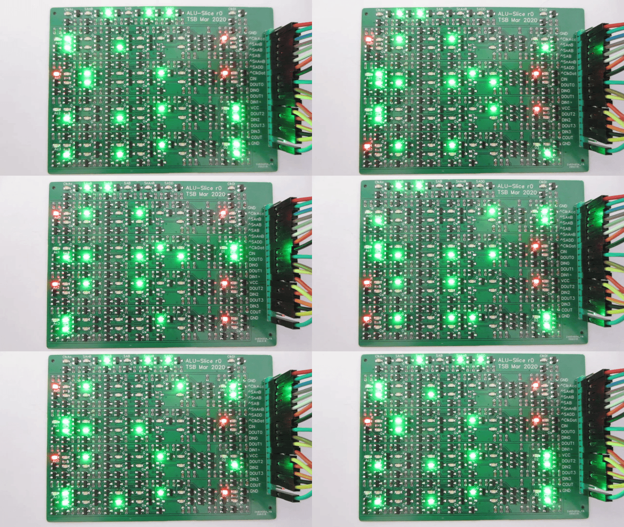
    Finally, the ALU board in action, repeating a sequence of ADD A,3 and NEG A:
  • ALU board PCB Design

    Tim03/18/2020 at 19:22 0 comments

    The ALU board is quite a bit more complex than the datapath board. To still be able to meet a <10x10cm² footprint, the layout had to be densified compared to the adress-datapath board.

    The circuit of one slice of the ALU board is shown above. The number if dual-diodes is quite high in this design due to wide-input AOI gates used as multiplexers for the boolean units. The XNOR gate on the right side is based on a cross coupled transistor pair. No LED could be used here due to stacking of several PN junctions in the current path.

    Eagle was used for the layout, making extensive use of the block functionality. Since only a two layer PCB is used, a good strategy is needed to make the layout as tight as possible. 

    As a general rule, I used the front side for local interconnects and the power rails. Each slice was layouted with a fixed height of 0.65", which allows placing two gates between the power rails. Copper fill on both front and rear side is used for the ground plane. The rear side is only used for global routing (I/O and control signals).

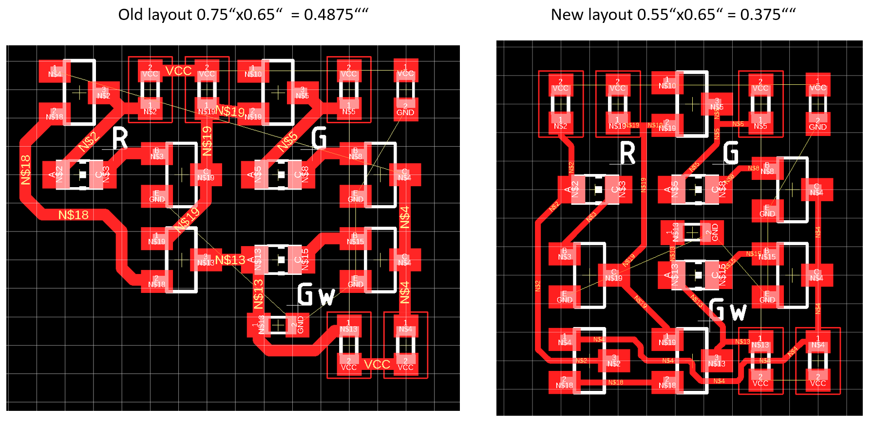
    After doing some estimations regarding copper line resistivity I noticed that it was possible to go to much smaller line widths.

    The image above shows a comparison of the old and new polarity hold latch layout. The new layout is much more dense and takes 30% less PCB space. One interesting observation was that going from 0603 to 0402 resistors did increase the layout area, since it was not possible to pass connections below the components anymore. Therfore I stayed with 0603 passives. Using smaller transistor packages was not an option either, since I was not able to source the transitor in a smaller package.
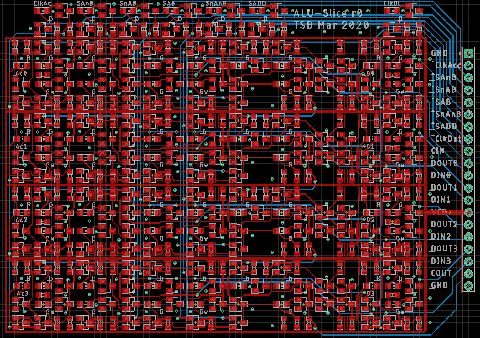
    The full layout, excluding ground plane, is shown above. Again, it was possible to fit four bit-slices on one board. In contrast to the previous design, I decided to include buffers for the control signals, located at the top. The fan out of the clock signal on this board is 8 gates. Combining several boards requires a clock tree for proper drive-ability.
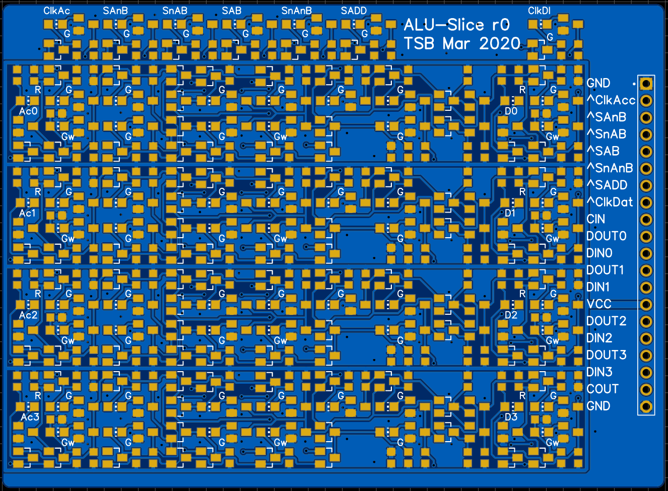
    The total PCB size is 10x7 cm², only marginally larger than the adress-board. Due to the more dense layout it contains 379 devices (75xT, 95xD, 67xLED, 122xR, 20xC) , 41% more than the datapath board.

    Board render is shown above. The populated boards should arrive in a few weeks.
  • The data-datapath design

    Tim03/04/2020 at 06:25 0 comments

    Time for another update. Mind you, at this point I am not documenting work that was already done in the past, but am following my actual development in real time. Therefore updates will be spaced much further apart, depending on how much time I can devote top this project.

    After finishing the adress-datapath design, it is time for the data-datapath.

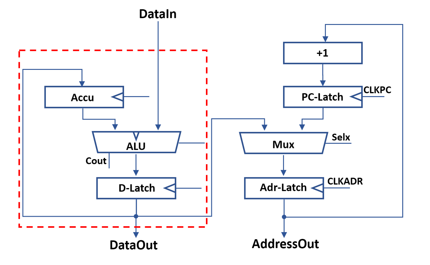
    The data-dapath encompasses the left side of the system design. The original M-CPU ALU was rather simple and only supported the two operations that were needed directly by the ISA: (Y,Cout)=A + B, Y=A NOR B.

    However, I changed the datapath a little to allow use of latches in the design. As a consequence, all reads are directed through the ALU. Storing the accumulator to memory also requires data to pass throught the ALU. Therefore, in addition to the operations above, also Y=A and Y=B have to be supported. When looking at the detailed logic, this adds quite some overhead.

    I lot of deliberation followed, also considering to merge accu+data latch into one edge triggered register as done in the original MCPU. The problem is, in that case an additional data input latch has to be added to the address-datapath. In the end it turned out to be more part-count efficient to stay with the latch based architecture.

    Two different designs were evaluated in detail.

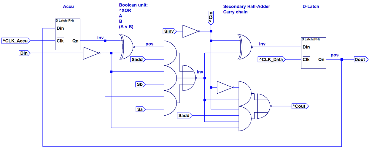
    A first implementation option for a single bit of the data-datapath is shown above. This design implements a full adder consisting out of two XNOR2 gates, an inverter and an AOI2 gate. Y=A/Y=B/Y=A OR B is realized with an AOI3 based multiplexer in the first stage. The carry line can be fixed to zero or one by using the Sinv and Sadd control inputs. This allows configuring the second XNOR gate to invert the result, resulting in Y=A NOR B.
    The table above shows the individual component usage. The total part count for this option is 80 per bit.
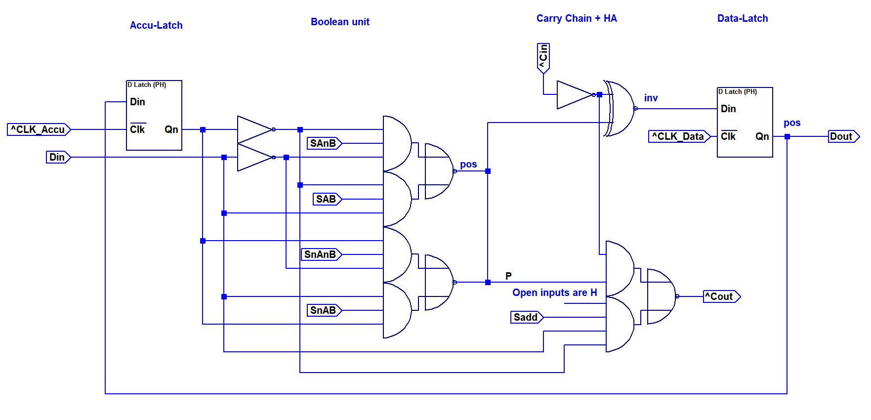
    The second option I looked into is a bit more universial and uses an AND-OR-INVERTER based multiplexer for the first stage of the ALU. (EDIT: 20/03/28, updated to fixed version.) By using the four control signals, it is possible to generate any boolean functions, offering the possibility to extend the instruction set of the CPU at a later time. This design is, of course, heavily inspried from the MT-15 ALU. Since the first stage is now also able to implement NOR, it was possible to remove the Sinv control signal. Instead only Sadd is present, which will inhibit carry generation if set to 0.

    Component requirements are shown in the table above. The total number of components is 82, only two more than the less versalite first option. Therefore I elected to go with this option, since it allows more flexibility.
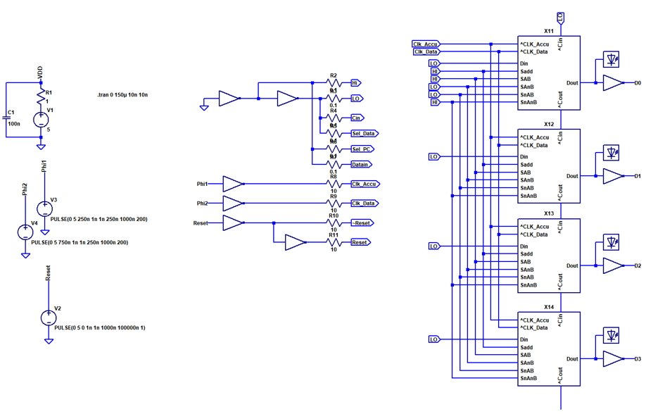
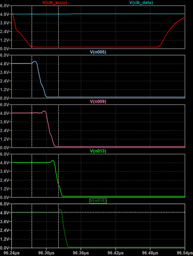
    The design functionality was tested in the test bench above.

    The image above shows carry propagation through all stages. The carry is low active. The carry propagation delay is approximately 11 ns per stage (45 ns total for 4 stages). Although this will propably increase in the real circuit due to more parasitics, it is a very reasonable result and suggests that an acceptably high clockspeed can be achieved even without resorting to a more elaborate carry chain architecture.
  • Blinking action - testing the hardware

    Tim02/22/2020 at 17:17 1 comment


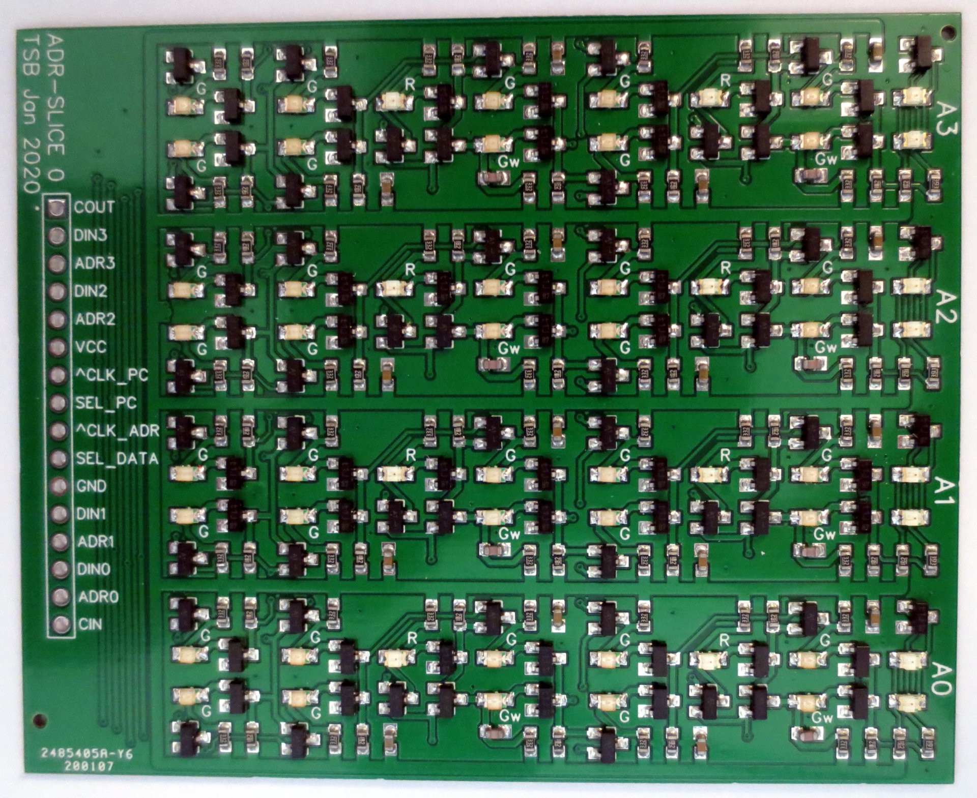
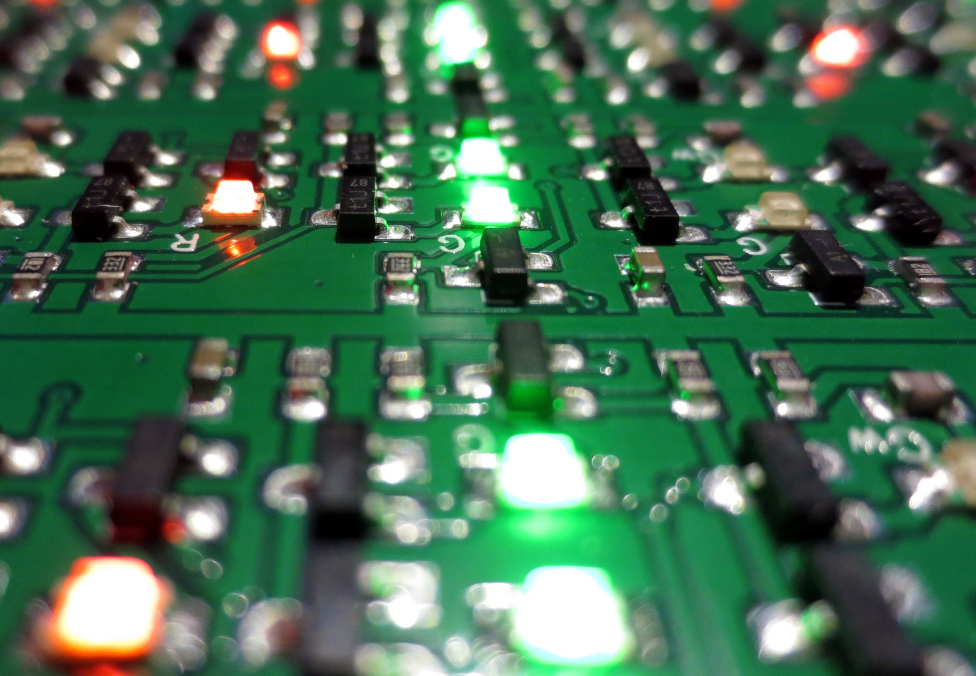
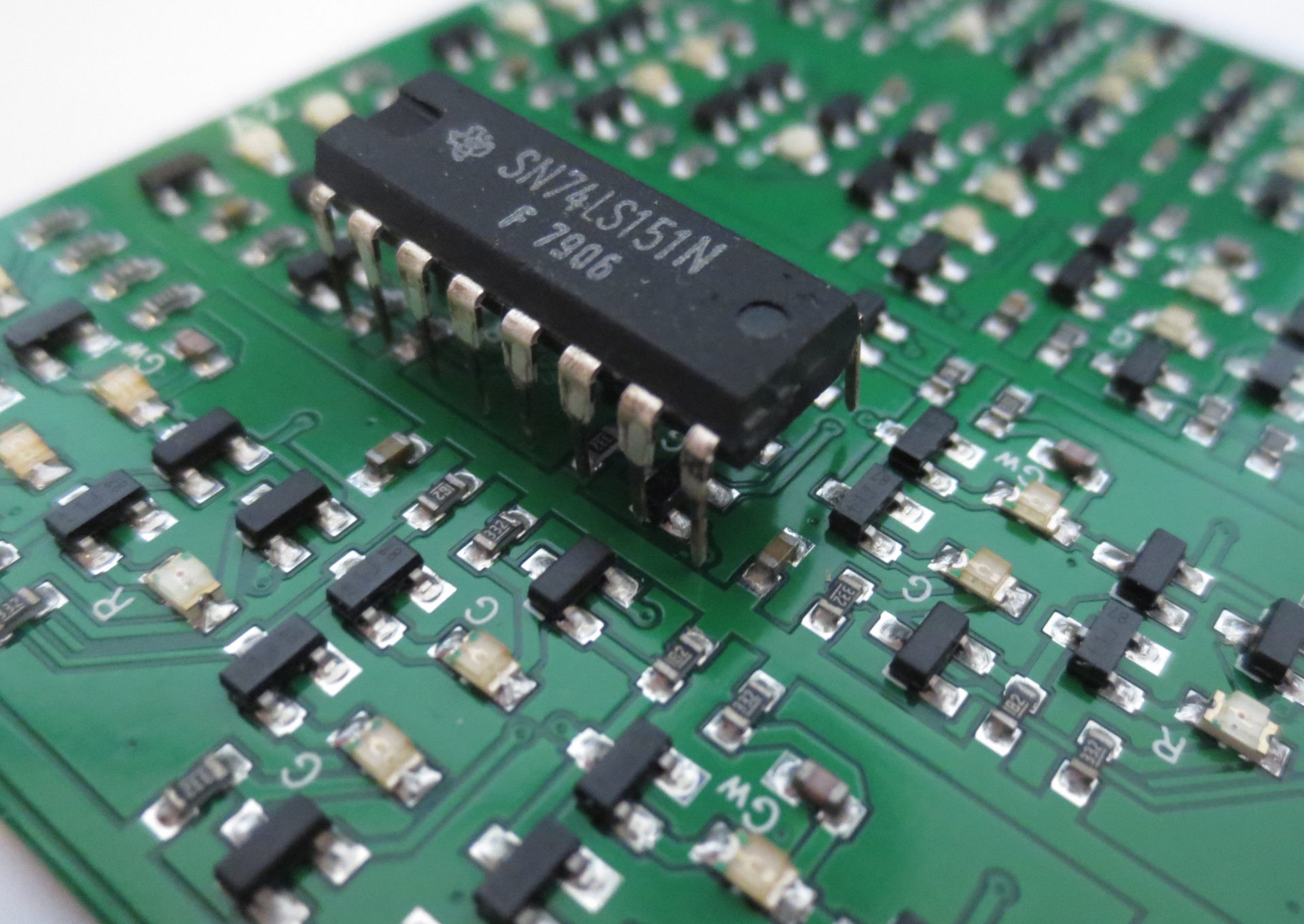
    Above you can see the an image of the hardware while it is operating. The red LEDs are part of the low threshold gates in the latches, while all other gates use green LEDs to set the threshold to ~2.3V.A size comparison with a TTL ICs. The gate density on the PCB in NAND equivalants is slightly lower than what would be achieved with 7400 NAND gates. Something to be addressed for later iterations...
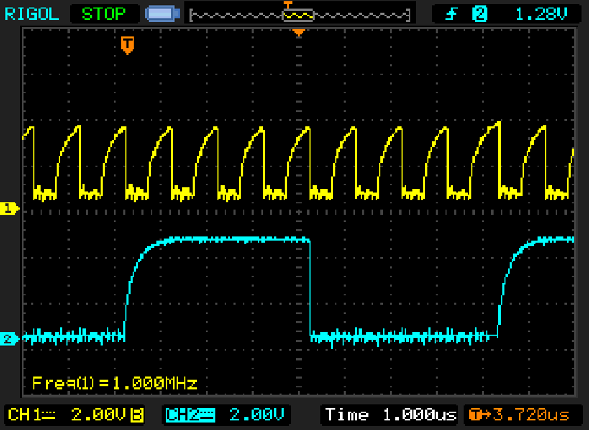
    The scope image above shows the A0 and A2 output of the address unit with SEL_DATA=0 and SEL_PC=1. In this configuration, the PC is increased with every clock cycle. Here, a clock of 2 MHz clock was applied. Operation was also successful at 4 MHz. I was not able to test any higher due to limitations on the generator side. Obviosuly this would reduce when more 4 bit slices of the adress path are combined, because the length of the carry chain would increase. One can see from the signal shape that the operating speed is very much limited by the rising edge. Right now, the collector current is limited to 2mA. Increasing the collector current further would allow even higher clock rates at the expense of power. Introducing push-pull output drivers may also be an option.

    Finally some blinking action, clocked at 2 Hz! Higher resolution here. The red LEDs on the left side of the PCB indicate the state of the address lines and are not part of any gate. You can see how the PC is counting up.

    Btw, only after looking at this animation, I realized that the fast (red) gates actually reflect the output state of the latch, even though they are not connected to the output. So, next time I can omit additional indicator LEDs.

  • Address-Datapath PCB Design

    Tim02/22/2020 at 11:25 1 comment

    Designing PCBs with regular structures using free tools turned out to be surprisingly tedious. In the end I used the free version of Eagle due to it's block feature which allowed replicating of circuit and layout units. The other options I looked at were EasyEDA and KiCad.

    Unfortunately, the free version of Eagle is limited to a single sheet, so I ended up transferring my nice hierachical LTspice implementation into a single paged mess of a schematic. The image above shows a one bit slice.

    Curiously enough, none of the many LEDs in the LTL gates represented the actual state of the address output pins. Therefore I introduced two additional indicator LEDs.

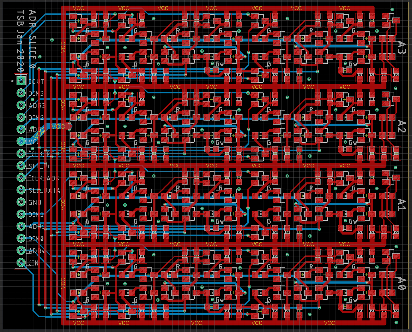
    The final PCB layout is shown above. I managed to fit a four bit wide slice of the adress path into one 8,5x7cm² PCB.

    A populated PCB is shown above. Since I am not too fond of placing all those parts by hand, I used an SMD assembly service. The finals stats are: 52 transistors, 48 diodes, 24 capacitors, 56 LEDs and  88 resistors.
  • Design of the address-datapath

    Tim02/22/2020 at 10:29 3 comments

    Implementation of the address path is straightforward based on the previously designed gates.

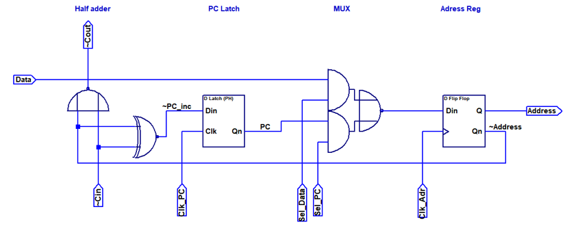
    The first design of the adress path is shown above. A half adder is needed to increment the PC. Since the gates are relatevely fast, I used a ripple carry adder. There are two latches for address and PC respectively. An AOI2 gate is used as multiplexer between PC and external address. The address latch can be loaded with zeros by pulling both control inputs of the MUX to low. This can be used to reset the PC.
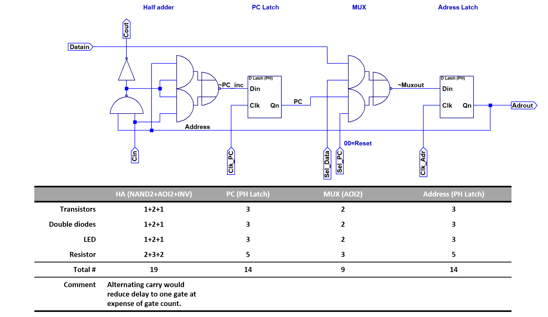
    The image above shows the design after some optimization to reduce part count. Each slice consists of 12 NAND equivalents and 56 components total. Note that the carry delay was increased to two gates.
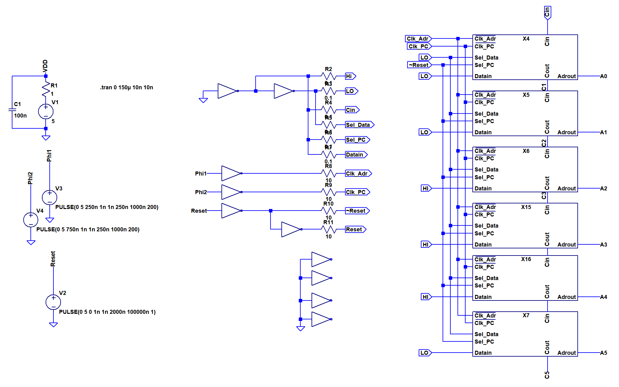
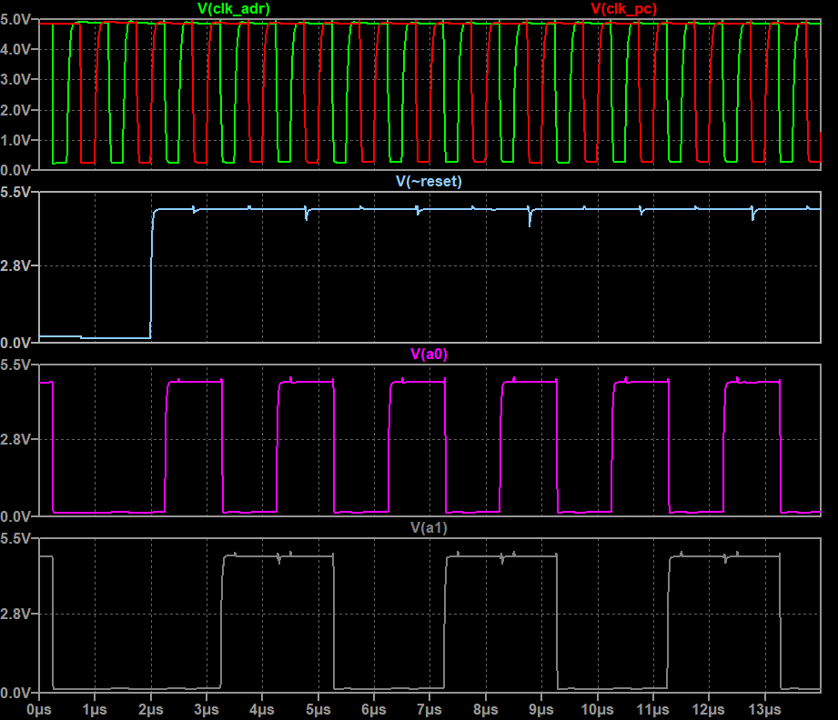
    Six of the bit slices were combined in a testbench to test the design of the full width datapath. A two phase clock is needed to alternatingly clock both latches. In this setting the circuit is configured to reset the PC and then increment it with each clock cycle.

    Output traces of clock, reset and the first two output bits are shown above. Everything works nicely.

  • The Architecture

    Tim02/22/2020 at 00:17 0 comments

    Now that all the gates have been designed and tested, let's discuss the CPU architecture. I spent quite some time pondering about a minimal architecture that is catered to a LTL implementation. To make a long story short: I essentialy ended up at the MCPU architecture again.

    There are some ways to simplify the ISA or the datapath, for example by replacing the ADD instruction with something else (think Brainfuck) or reducing datapath width. All of these lead to an explosion in number of instructions needed to perform even the simplest operation, which will in turn increase memory size requirements and hence address path width. A nice example of this extreme are designs like the Qibec, which is a very nicely done implementation of an "invert bit and branch" one bit OISC. While it reduces the datapath to one bit, the address path needs to be increased to 16 bit to allow any meaningful program.

    I may rant more about this at a later time, but in essence there seems to be little overall gain for these trade offs and all of them come at a great disadvantage in usability of the instruction set architecture.

    I noticed way too late that I was actually not the first to implement the MCPU as a discrete CPU: The ED-64 is a very great looking implementation based on core memory. Kudos to Andrew for this great effort!

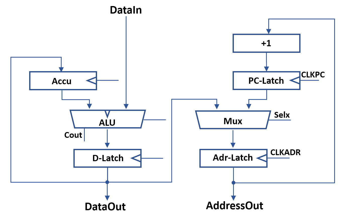
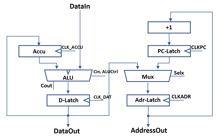
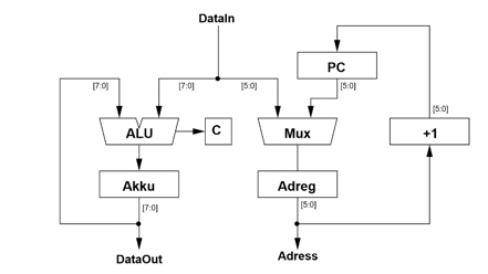
    The original MCPU architecture is shown above. There are separate flows for the address and data-path. The state machine is not shown. Since this design is catered for a CPLD, it assumes edge triggered flip-flops for all registers.

    The MCPU programmers model is based on two registers: Accumulator and PC. The ISA consists of four instructions in a fixed encoding that is based on a two bit opcode and a six bit memory address. This ISA can be directly mapped to the datapath shown above with minimal control overhead. See MCPU link for more information including assembler, emulator and example code.


    In LTL it is much simpler to use latches instead of edge triggered flip flops. Introducing latches requires changing the design in some places to avoid race conditions where the input of the latch is dependent on its output. This is, for example, the case for the accumulator. The diagram above shows a latch-based architecture. The main modification is the addition of a data latch. The data latch is used to prevent race conditions for memory loads and accu-accu operations.

    For implementation, I divided the design into three sections: The address path, the datapath and control. This modular architecture allows some freedom to modifify the CPU at a later time and add more instructions. Both data paths will be implemented in a bitslice architecture. This allows reconfiguring the CPU from 8 (data)/6 (address) to other configurations like 16/12 by just adding more slices.

  • Flip Flops / Latches

    Tim02/19/2020 at 20:23 4 comments

    Now to the last category of building blocks: Flip Flips.

    If you grew up learning about digital electronics in the advanced CMOS era, like me, you will most likely be accustomed to using edge triggered flip flops for everything. Unfortunately, it turns out that proper edge triggered flip flop require at least 6 NAND gate equivalents, unless you have dynamic CMOS logic at your disposal.


    For those of us who were suddenly beamed into the discrete LTL age, latches are a much more part count efficient solution, as they only consume about half as many components as a static edge triggered flip flop.

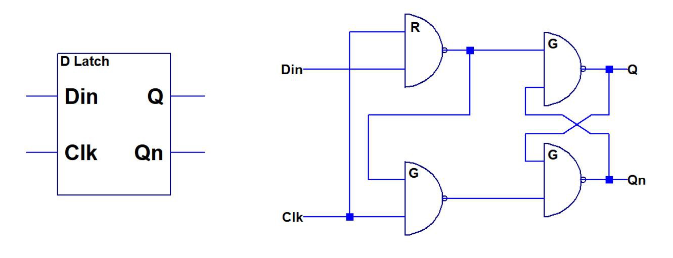
    A commonly known minimal representation of a gated D-latch in NAND2 is shown above. See also Wikipedia article. A nice propery of this design is that it only requires a single clock input and has both inverted and non-inverted data outputs. Data from Din is forwarded to the output while Clk is high. The state of the latch is frozen on the high->low transition of the clk and held while clk is low.

    When using this design in high speed circuits it becomes apparent that it has a nasty habit of generating glitches. The origin of this effect is the NAND2 gate in the lower left. The clock signal arrives on one input directly and on the other it is delayed through the NAND2 gate in the top left.

    This effect can be somewhat reduced by tweaking the propagation delay of the logic gates. In LTL this is easily possible by changing the LED color to change threshold voltage. In this case I introduced a faster "red" (hence the R) gate with lower threshold as the top left gate.

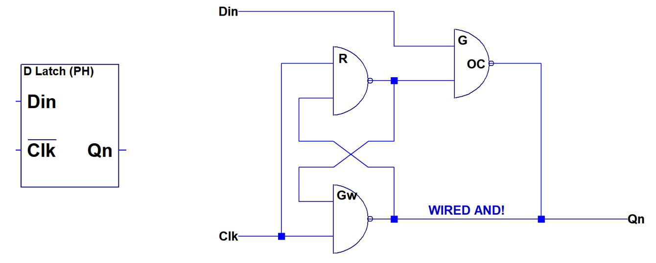
    There is also a way to reduce gate count to three by replacing one of the NAND2 gates with a wired AND. This is described in a now expired patent. (A similar design is described in this patent)
    The patent also describes to work around the aforementioned glitch by introducing one faster gate. A disadvantage of this design is that it is only has an inverted output. The clock input is also inverted compared to the previous design: Data will be forwarded for clk='0' and held for clk='1'.

    One very important point of learning came out of actually simulating a full design including the latch and observing dynamic operation. To do this, it is necessary to perform a transient simulation in Spice - LTspice was used here.

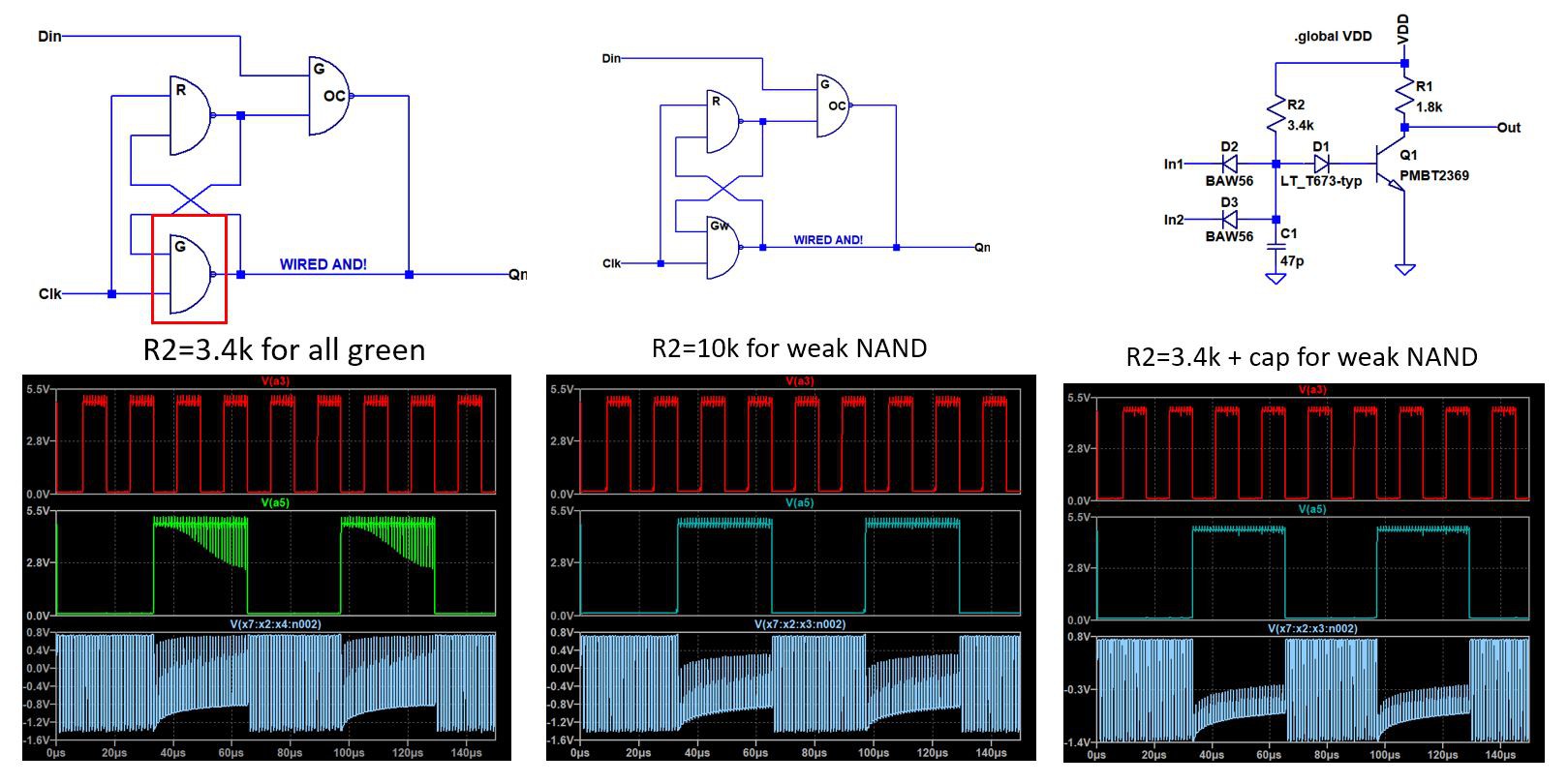
    The figure above shows simulation results and modifications to the latch design that were applied as a result of the observations. The latch was used as part of a program counter here. The first line (in red) of the simulation traces shows the fourth bit (A3), the second line shows the sixth bit (A5).

    The leftmost column shows the results of the unmodified circuit. A3 looks nice and clean. However, A5 shows a series of negative spikes when the output is high. Interestingly, this behavior changes over time. It should be noted that this is mostly a cosmetic issue at this point, because the glitches are far away from the clock edge were the data is latched. Elminitating this effect should still be a priority as the additional noise may snowball into actual bit errors when the timing gets more tight.

    The culprit is the gate indicated by the red box, which receives a clock signal that is partially delayed by another gate. The lowermost trace shows the node directly at the base of the gates transistors. This node is basically floating when the gate is turned off, since both the LED and the base junction are reverse biased. You can see that it assumes a deeply negative potential. It appears that some of the charge on the node trickles away over time, making the gate more sensitive to spikes on the inputs.

    A solution to this issue is to make the gate in question "weaker", so it becomes less sensitive to transient conditionts at the inputs. I tried two ways of doing so: Increasing the base resistor (middle column) and by adding a small capacitor (right column). Ultimately I settled on the additional capacitor, because increasing the base resistor would reduce the current...
    Read more »

View all 16 project logs

Enjoy this project?

Share

Discussions

Ken KD5ZXG wrote 11/30/2023 at 03:41 point

If backplane obscures LEDs, might bring to the edge with lightpipes. Would that want a small mirror above each LED? Could pipe cut at an angle be mirror or prism enough? 

  Are you sure? yes | no

Tim wrote 12/03/2023 at 09:11 point

That would be an aweful lot of mirrors :) It may be simpler to use a video camera and a display?

  Are you sure? yes | no

RunnerPack wrote 12/05/2023 at 14:09 point

Light pipes don't need mirrors. Simply incorporate a polished, angled surface, and the refractive index mismatch will ensure reflection (see: total internal reflection, aka TIR)

  Are you sure? yes | no

Ken KD5ZXG wrote 01/08/2022 at 07:40 point

4way LUT XOR'd against the prior slice's carry looks good. Not so thrilled by ripple carry. Combinatorial works fine for exceptions that replace carry, but search you some "Muting Transistors" and propagate Manchester pass-though style. 

  Are you sure? yes | no

Rudraksha Vegad wrote 12/18/2021 at 19:59 point

😍😮😲😵 WOW!!!!

  Are you sure? yes | no

Alvaro Barcellos wrote 05/03/2021 at 00:29 point

beautiful

  Are you sure? yes | no

Mark Jeronimus wrote 06/24/2020 at 20:55 point

> I still have no idea how to do it in a way that does not obscure all the nice LEDs

Take an example from the Megaprocessor :]

  Are you sure? yes | no

ExplodingWaffle wrote 03/28/2020 at 18:19 point

this is peak blinkenlights, i love it

  Are you sure? yes | no

bobt1864 wrote 03/04/2020 at 22:34 point

Hi Tim, some comments from a grey haired analog electronics engineer, as one of our uni lab projects, we had to build a simple CPU on a massive patch panel, by plugging in leads all ove the panel, your project reminds me of that.

(a) you should be using base pull down resistors, your slow pull up on the outputs is caused by the miller capacitance between b and c .

(b) google up apollo guidance computer, it used similar logic building blocks, and "wired-or outputs", you might learn some tricks from them. 

(c) Your schematic would look a lot neater, and quicker to draw, if you used the Vcc and gnd components. also if you create components for red and green LED's and color the triangle in each component red or green. 

(d) you can get two transistors in one SOT23-6 package , you can use the other transistor as a diode if needed, or not at all if the track layout is too tricky, you could use the same device as two diodes to replace the BAW56, you could use two transistors to make a multiple emitter transistor like used in TTL (or multiple base, or multiple collector). You can get resistor arrays in a 1206 package too, you don't have to use all the resistors in a package, just using two resistors is less space than 2 x 0805 packages, and you can go series and parallel so a quad 4k7 package can be 2 x 4k7 + 2k3  OR  2 x 4k7 + 9k4 OR 2k3 + 9k4  It is a lot simpler to assemble a project where have fewer line items in your BoM.  A lot of my designs for example use 2n7002 to switch relays, and a diode connected 2N7002 across the relay for back EMF suppression. (Also the base-collector diode of a normal transistor is much lower leakage than a normal diode, so can be used with say a 2n7002 and a  10uF/10Meg RC timing circuit to get 2 minute delays.)

  Are you sure? yes | no

Tim wrote 03/06/2020 at 07:51 point

Hi Bob,

thank you very much for your insightful comments. These are interesting questions indeed.

a) I don't think the miller capacitance plays a large role, since the hfe of the transistors is not that high (~100), Cc is low (~4pF) and a relatively high base current is used. I will try to add some simulation traces of the switching operation in detail. The secret sauce is the choice of the transistor, which I outlined in detail here: https://cpldcpu.wordpress.com/2020/02/14/what-made-the-cdc6600-fast/

b) Thanks, that's a good tip. It uses RTL ICs if I remeber correclty?

c) Well, the circuits are coming directly out of LTSpice. There are limited options of changing the look.

d) That's an interesting point. I will outline my layout and component choice in a bit more detail, some things are quite counterintuitive. For example usage of smaller resistors resulted in larger layout due to routing constraints (no traces below resistors). Also, the assembler charges per pin, not per component, so they bizarrely encourage use of more parts. I like the idea of using arrays though, have to look into this for the next design stage.

  Are you sure? yes | no

Yann Guidon / YGDES wrote 02/19/2020 at 15:08 point

We request, no, we require a video !

As well as an exposé of the architecture of your computer :-)

  Are you sure? yes | no

Tim wrote 02/19/2020 at 18:54 point

It's already done, I only need to write it up.  :)
Everything sequentially in order, as I cannot switch project logs around

  Are you sure? yes | no

Yann Guidon / YGDES wrote 02/15/2020 at 21:21 point

Oh my, you ARE a true TTLer indeed !

  Are you sure? yes | no

Peabody1929 wrote 02/15/2020 at 18:07 point

Would you do a comparison to TTL logic as well?

  Are you sure? yes | no

Tim wrote 02/15/2020 at 18:18 point

Not sure in which way? The logic levels of the design are compatible, but the circuitry of the gate is, of course, completely different.

  Are you sure? yes | no

Dan Maloney wrote 02/15/2020 at 04:08 point

Promises to be irresistibly blinky. Looking forward to it!

  Are you sure? yes | no

Similar Projects

Does this project spark your interest?

Become a member to follow this project and never miss any updates