-
[L] Component alignment and solar pads
06/21/2023 at 15:41 • 0 commentsIt's been another 90 minutes and I've got some updates.
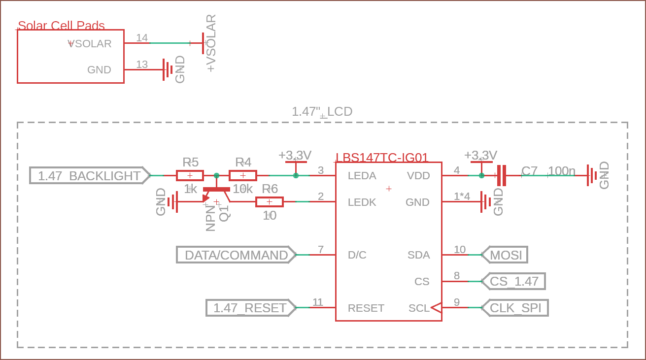
Just like with 3D CAD, I can have more than one symbol in a component. I still have the freedom to put each symbol in an arbitrary location:
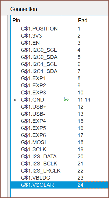
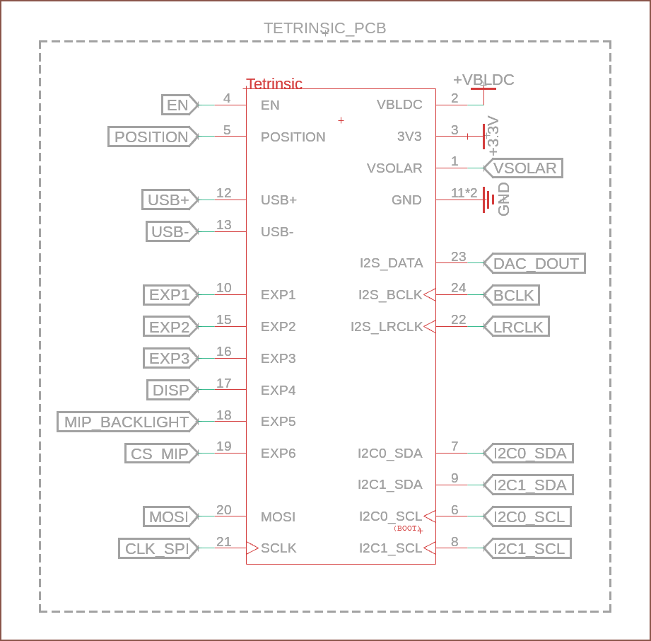
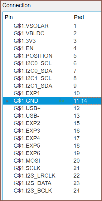
I've reordered the Tetrinsic masterpad so that VBLDC is on the right side. This also allows me to evenly split the EXP pins in half. I've put slightly lower importance pins on the right edges (POSITION / VSOLAR) in the event of manufacturing issues present at the edges of the PCB.
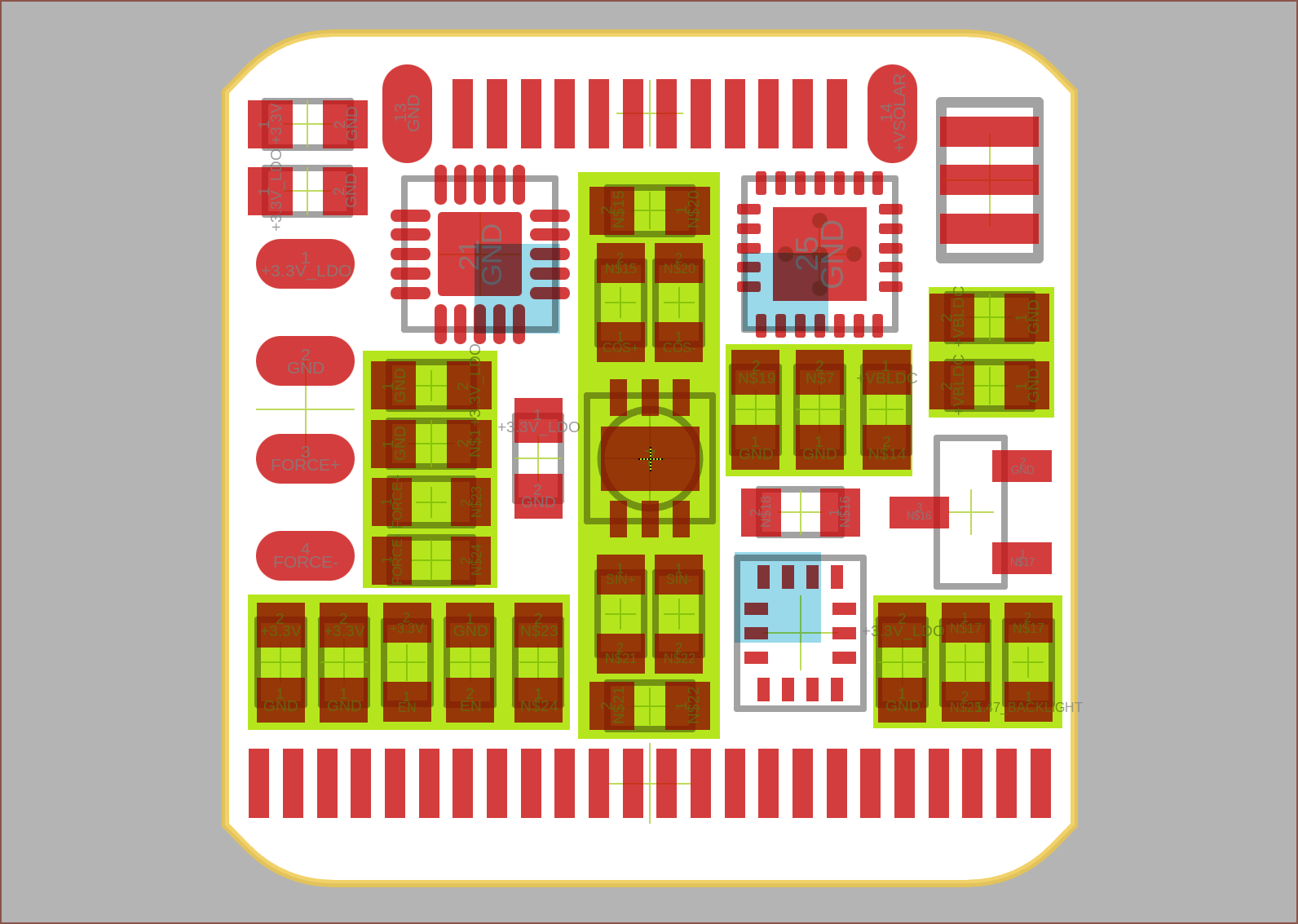
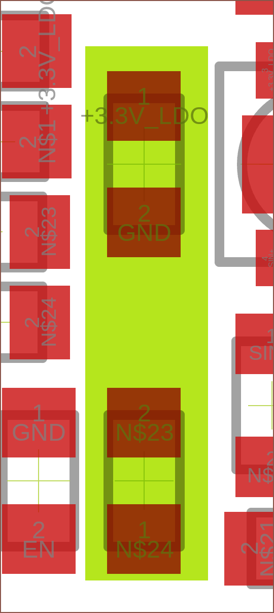
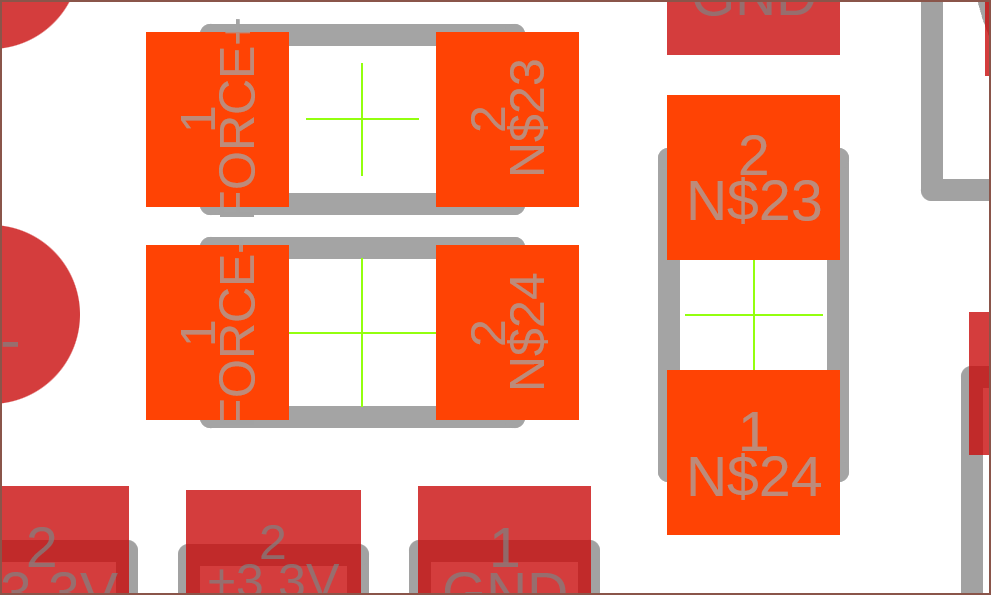
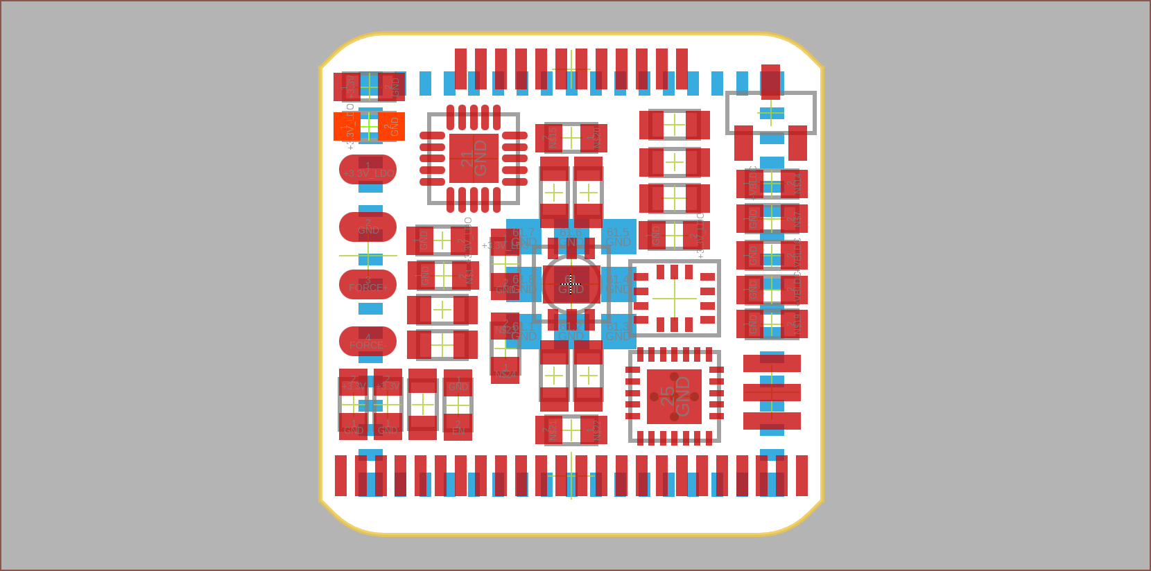
I've also been able to align components (green) and "circular pattern" the blue-marked corners of the ICs. This has the added benefit of the BLDC controller being reasonably far away from other ICs. However, it's reasonable to expect that I'll have to revert the position of the 2 passives shown below to make trace routing easier:
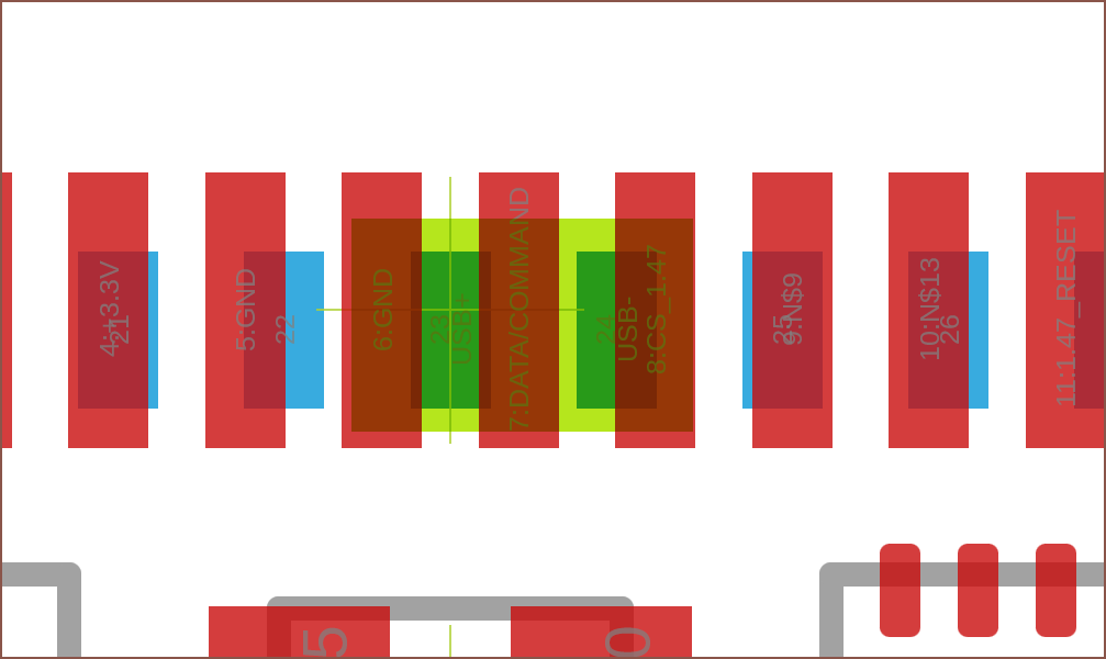
A lot of things, especially the USB data lines, are on the opposite side of where all the action is.
Thus, I think it makes the most sense to rotate 180...
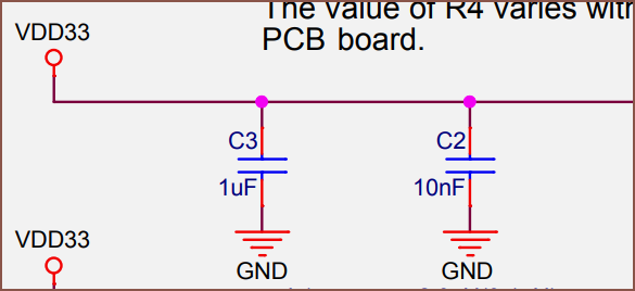
... and then swap the order on the masterpad. The drawback is that the S3-MINI's capacitors are now on the opposite side of the board to the 3.3V input. The docs don't really mention anything about this distance, and they're still close to the 3.3V input pin in the masterpad, so I'll chance it since there's a higher chance for USB interference than things breaking due to an imperfectly clean power to the chip. It shouldn't even be that bad, since the module itself has some:
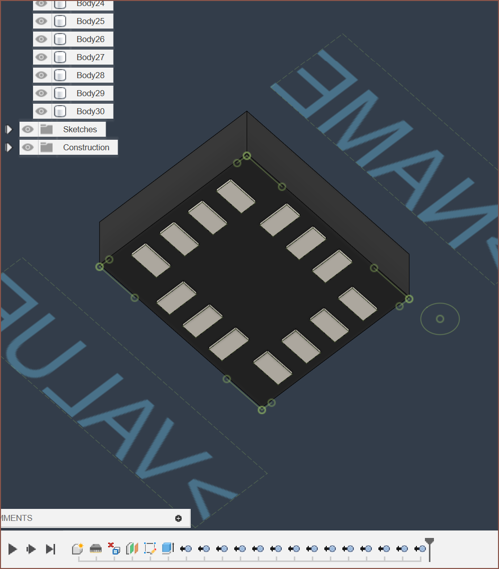
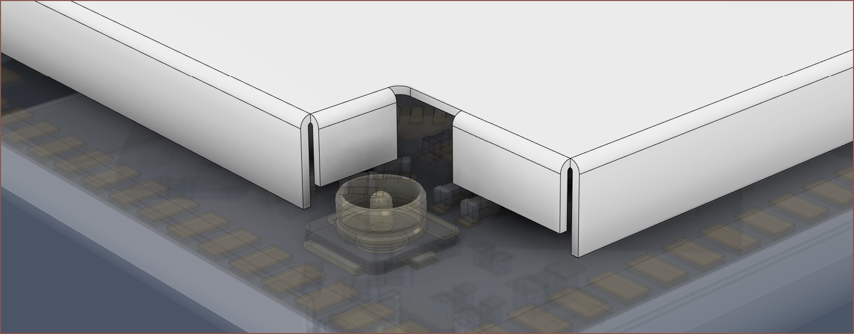
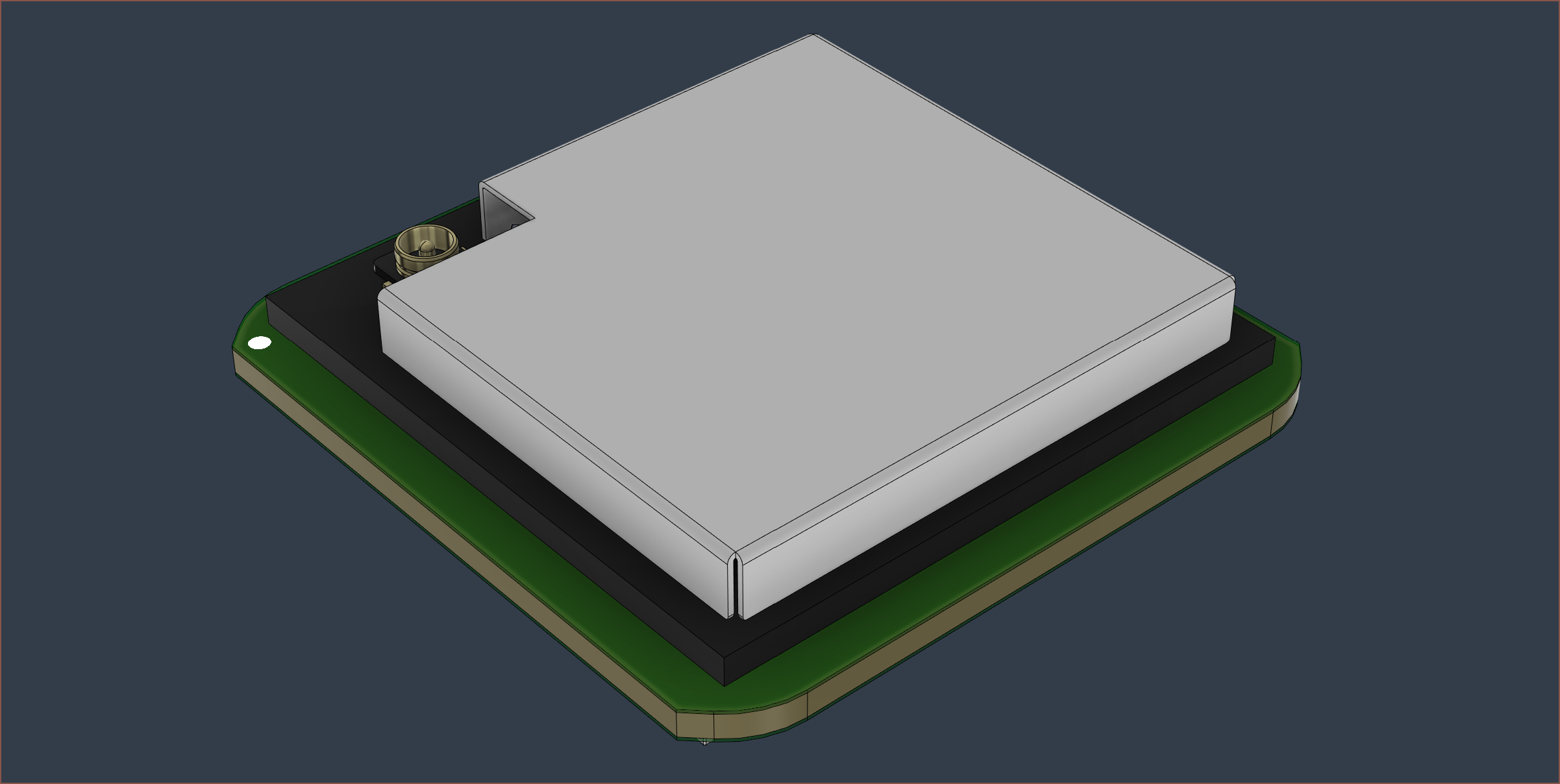
Oh, and not having these 2 walls of the MINI-1U has made me suprisingly annoyed, so I've finally spent a few minutes to model something. There's almost no images online of this angle so I'm just guessing.
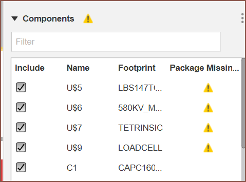
Also, Fusion is going to keep requiring me to check / uncheck if I want an auto 3D model generated.
Did some reading and it seems they never got anywhere with that, so I'm just making empty 3D models:
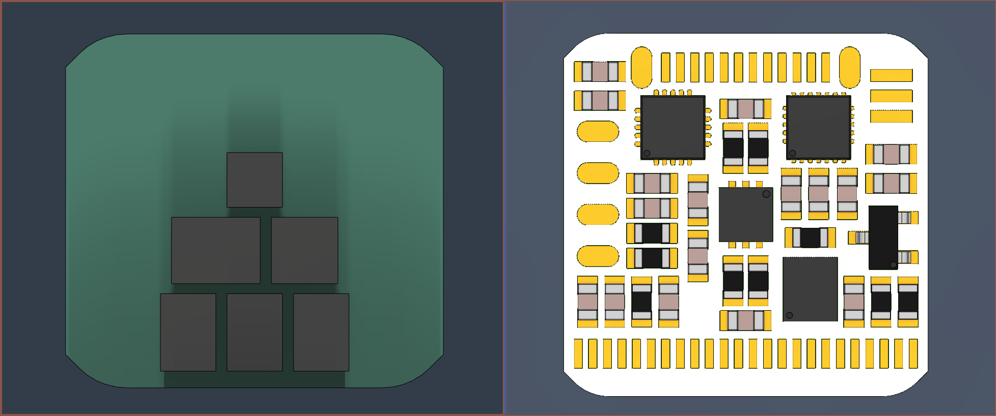
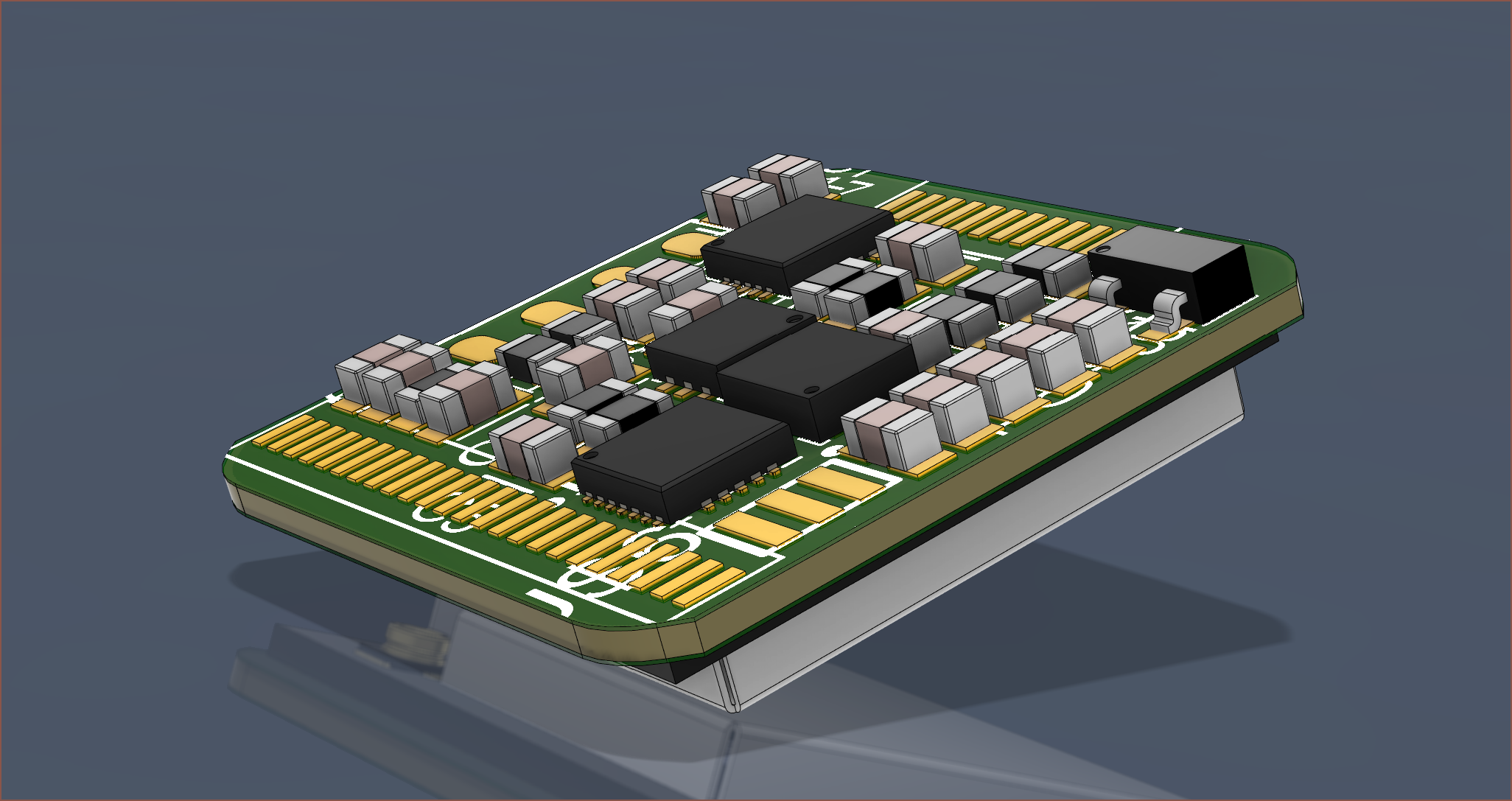
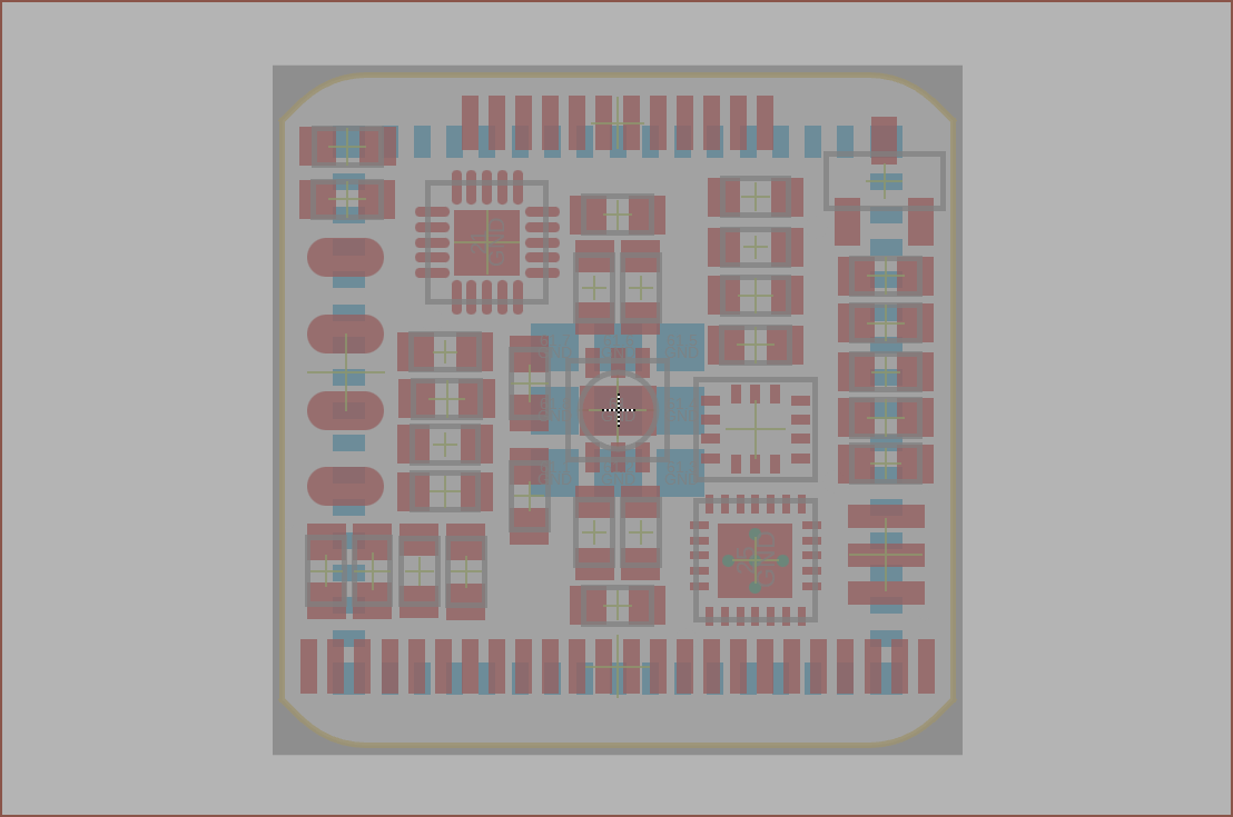
This PCB design is really giving me a throwback vibe when I thought I could get away with a 15 x 17mm PCB:
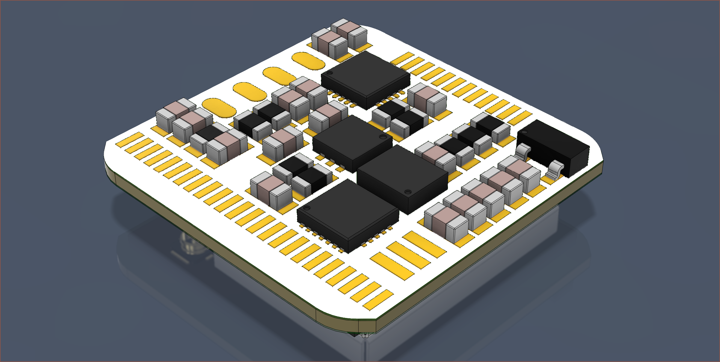
How it started (v97) verses how it's going (v285) It looks just as simple from the other side though:
No space for Tetrinsic branding, unless I laser etched the top surface of the shield. Actually, on second thought, I could always use a sticker like what is done for M.2 SSDs. I still feel like vias are going to mean that I have to make the board longer than what it currently is.
Time from starting this log to finishing: 2 hours. (So everything in this log is 3.5hrs of work in total)
-
[L] The start of the PCB
06/21/2023 at 03:02 • 0 commentsI modelled the 17.5mm square I wanted inside the main Tetrinsic file and then clicked through some menus to make it a PCB border. Then I linked the schematic:
The background music of my mind upon seeing all those passives: [00:00 - 00:12]
Me: It looks like space invaders! It's going to be near impossible to fit all those on!
Me, 2 hours later:
It suprisingly all fits, even when trying to keep bypass capacitors nearby to their respective chip. Obviously, this can all change once vias are introduced.
It's nice to see what a 3D version of the board could look like. I'm planning to coat everything in white silkscreen. Everything is so dense that there's really no point of marking anything.
Pardon?
Fusion 360 to the obvious line I was about to drive: [00:01 - 00:19]
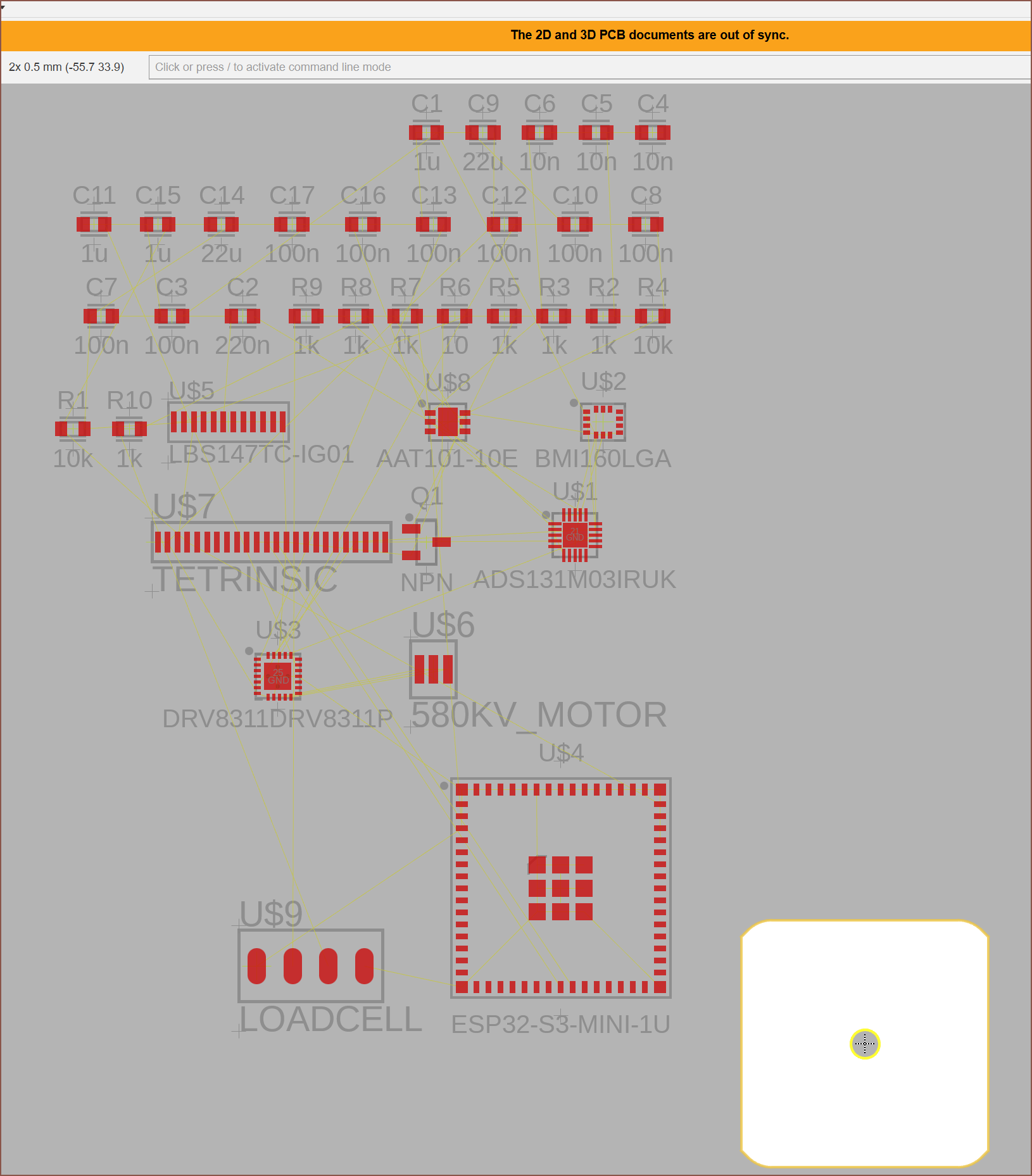
Ok an hour of research (to find out that this is a legit thing that Fusion 360 doesn't support even though why else would you derive a PCB from a sketch in the design??) and manually setting up a new link later... I've fixed it.
I've even figured out how to coat everything in silk:
I think leaving the other side as green is a nice contrast.
It slots into the available space nicely.
And now it's 4:40am, working on Tetrinsic for approx 15 straight hours.
-
[L] Updated Schematic with New Components
06/20/2023 at 22:47 • 0 commentsSo I've spent... oh it's 22:20 now and I started at 1pm... wow it's been over 9 hours?
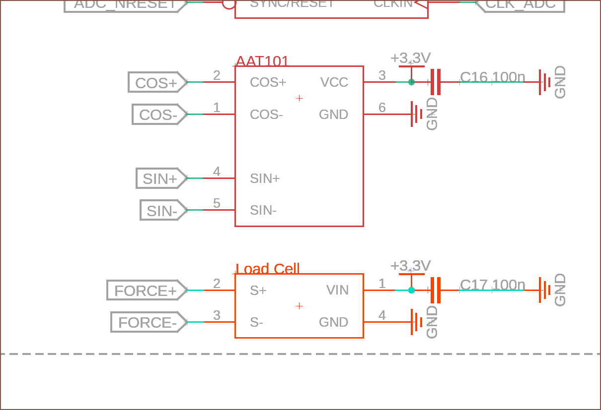
At this very moment, I've created the symbol and 3D CAD for the AAT101:
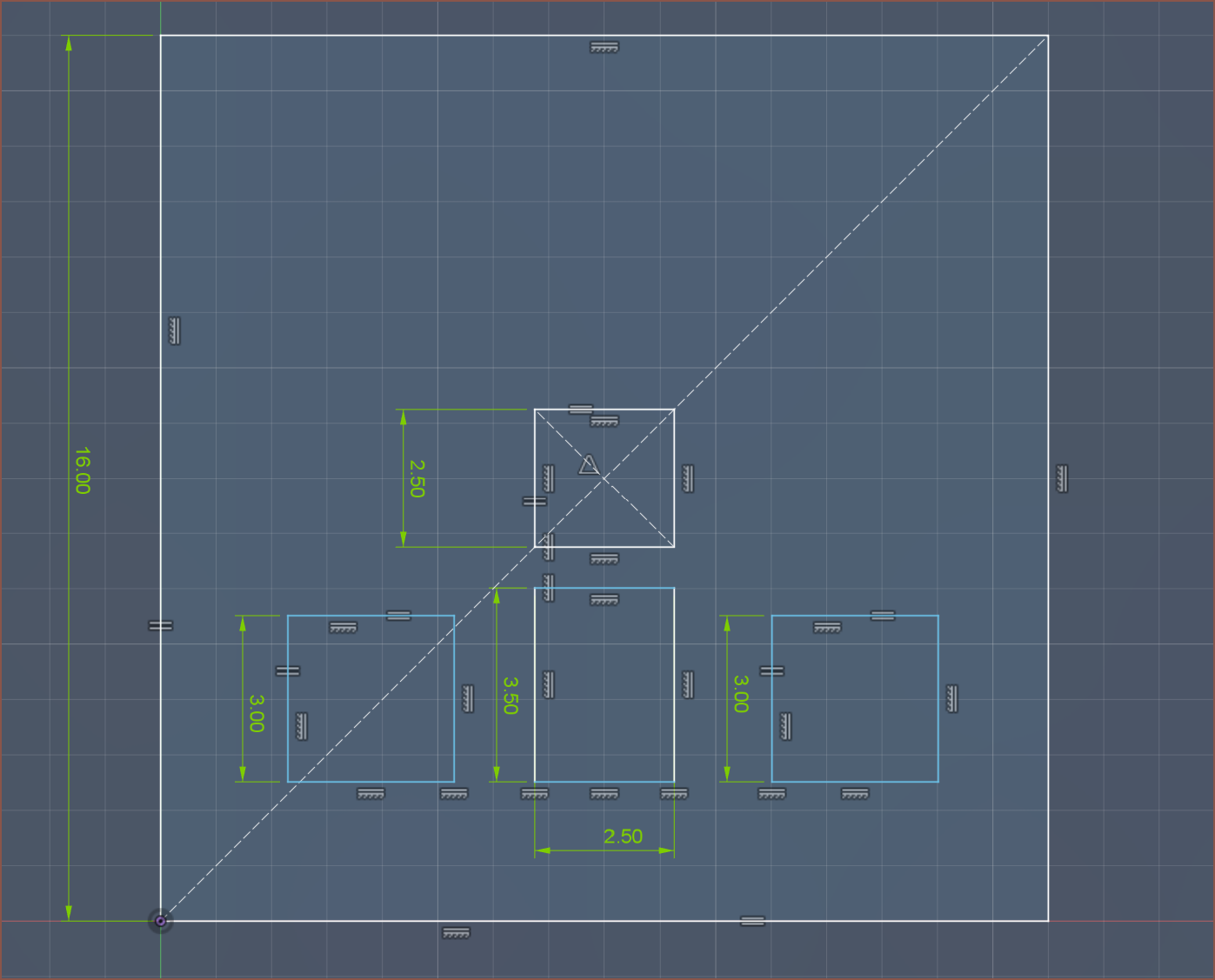
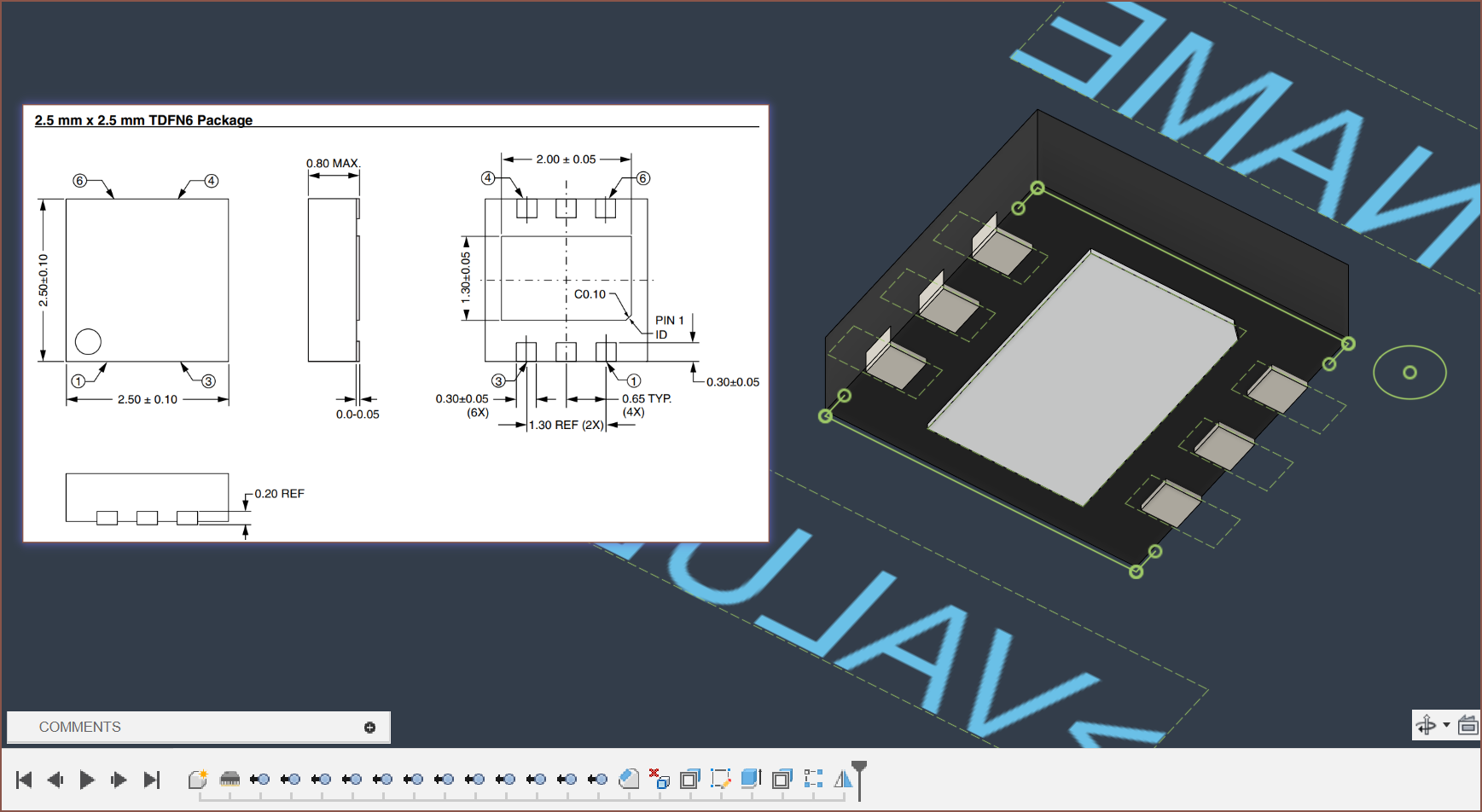
There's a Fusion360 bug where the pads won't generate correctly if the height and width are the same, such as this one. It'll be nice if there was some option to toggle rectangular pads like you can for the footprint.
I've now also created the pad for the load cell. I'll assume that a 2.54mm pitch is easy enough to work with, though I may need to shrink down if it's too large on the PCB.
Since the AAT101 is literally just a wheatstone yet specifies a 100nF capacitor in the BOM, I'm going to do the same for the load cell.
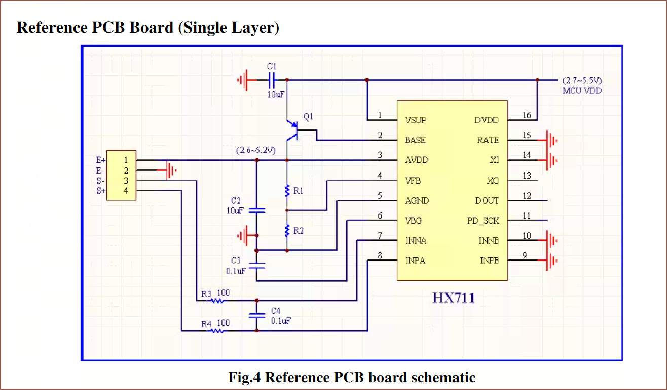
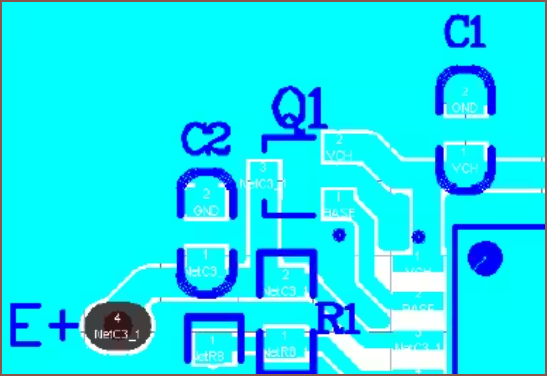
In this reference PCB I found, the bypass is even larger, but it's also connected to a chip so it's hard to tell if it's required for the load cell or not. It's location on the PCB (C2 in comparison to C1) suggests it is, though. Well as long as the pad is there, I can change it later on.
In other news, I've...
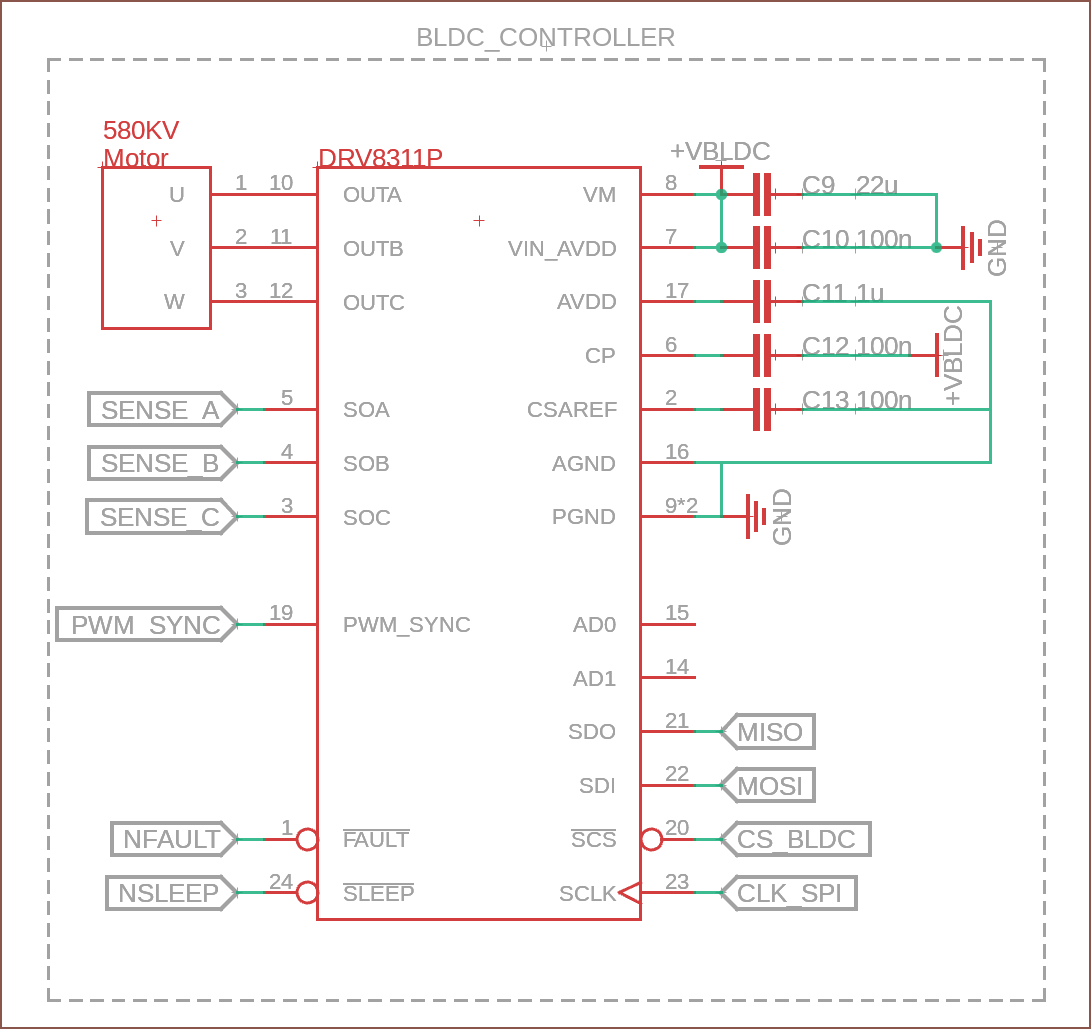
...wired up the BLDC:
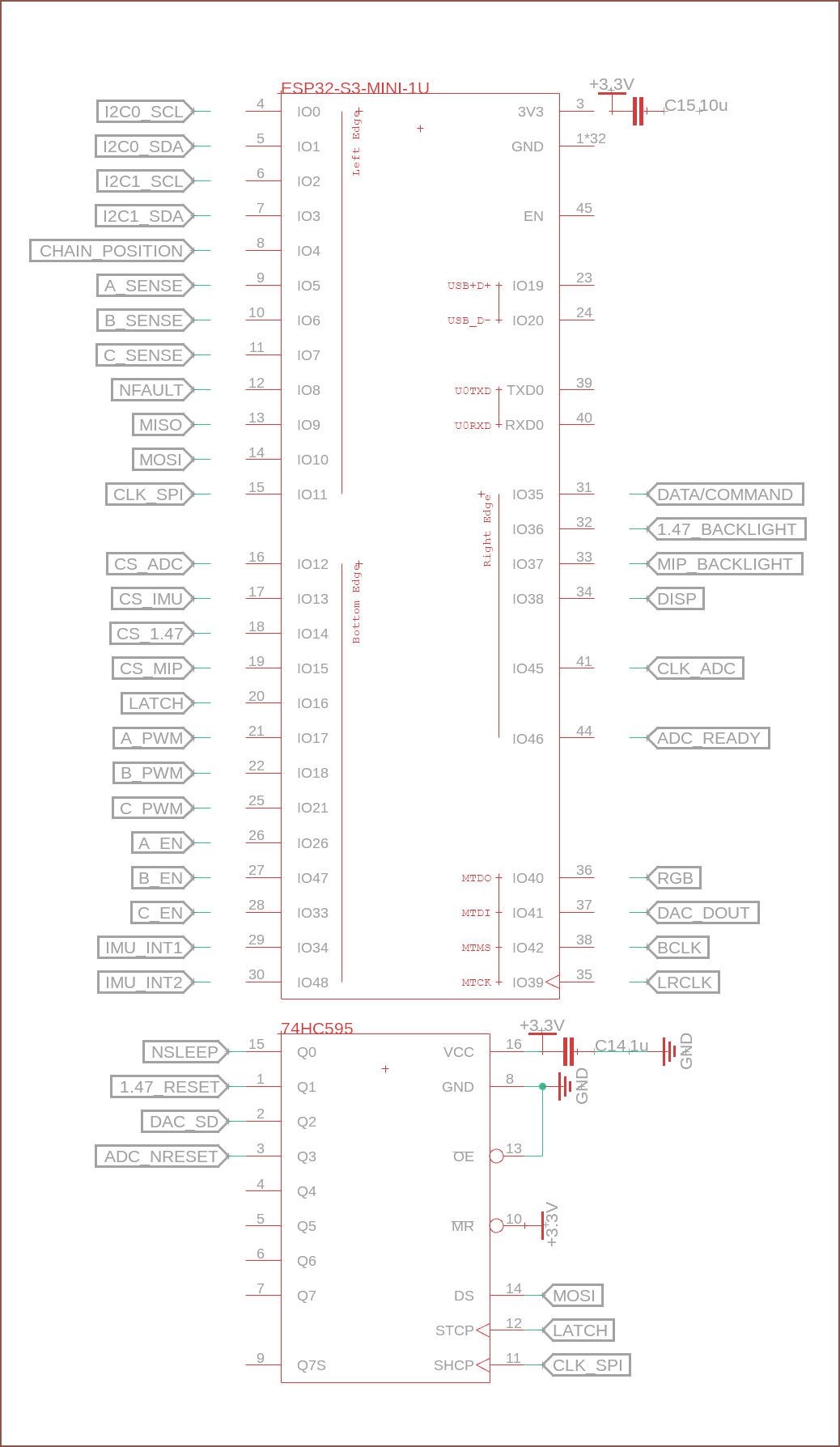
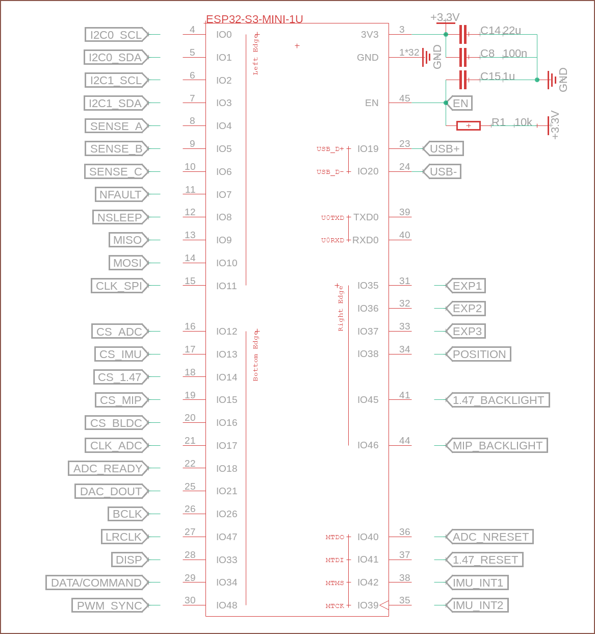
I still got to read up what ADn does. ...fit all the pins on the MINI-1U and removed the 595, as well as set up the power and enable pin (as per datasheet recommendations):
Quite a lot of my time was finding out if I should keep those TXD/RXD pins free. It seems that those are the pins you'd use to program the chip the traditional way (using a USB-to-serial debugger) but the ESP32-S3 docs say I can just use USB for that functionality (which also allows me to use the JTAG for IO). ...and set up a 24P 0.7mm FPC that will be equal to the width of the PCB (which should be 17.5mm):
The POSITION pin going to the Tetent PCB really makes things easier, as I can now just have a resistor chain that divides 3.3V into 8 different voltages (including 3.3V and 0V).
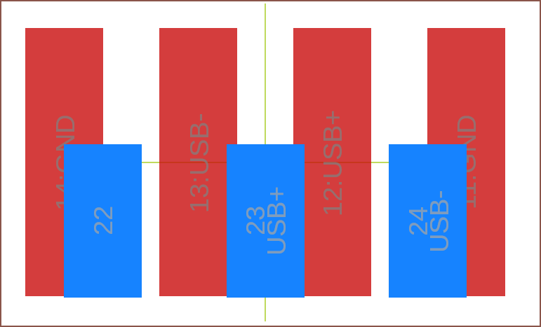
I2C0_SCL is connected to IO0, which is a strapping pin. If the pin is low after a reset, it'll go into boot mode. That's why there's a "(BOOT)" text under the pin.I've put 2 GND lines around the USB lines in hopes of reducing interference, imitating a shielded cable. Next Steps
Most of my research today has been around flashing multiple ESP32s. I know that there's an OTA thing, but does that mean I need to enable WiFi on all Tetrinsics momentarily? Another method could be exposing the TX/RX pins and having something like that GPIO matrix on I2C1 so that the Tetrinsic that is connected via USB can then program all the other ones
There's also the slight concern that IO3 is also a strapping pin and so it might not be a good idea to have it on I2C1.
As long as I don't burn any eFuses (which are things that can't be reset to a 0 if a 1 is written to it), I should be able to use it just fine. Actually, since it'll be connected to a pull-up (and GPIO3 is ignored if either eFuse 1 or 2 is a 1), I'd still get the USB Serial mode. Thus I don't have to worry about it, unless I need to use JTAG. I don't have enough pins for it to even be an option really.
But hey 🎉🎉that LOADCELL symbol/footprint is the last one I need for this PCB design. This is a milestone I didn't even acheive on the first schematic/PCB design.
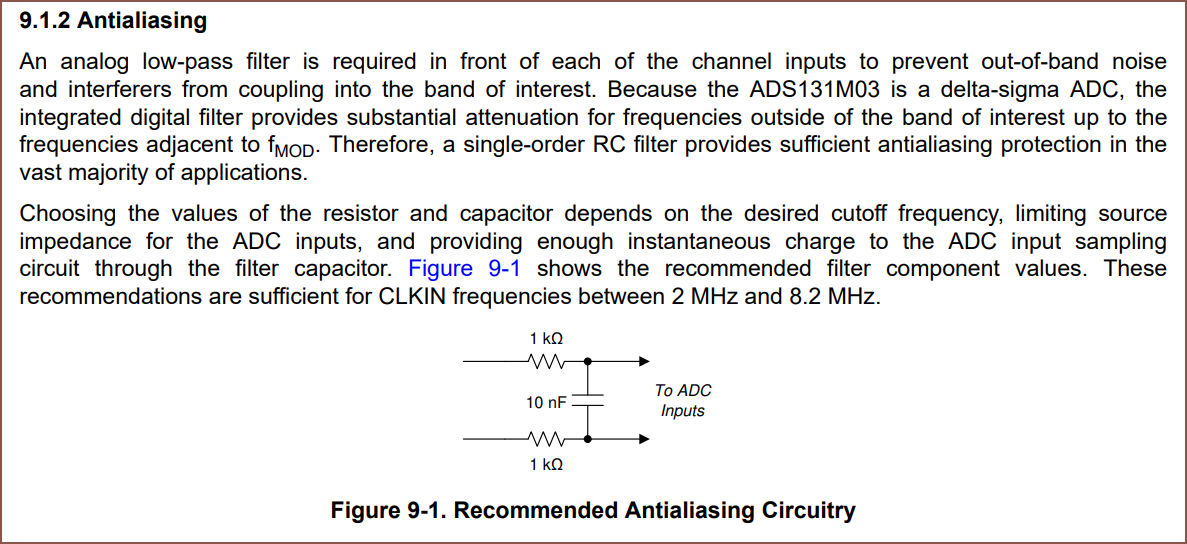
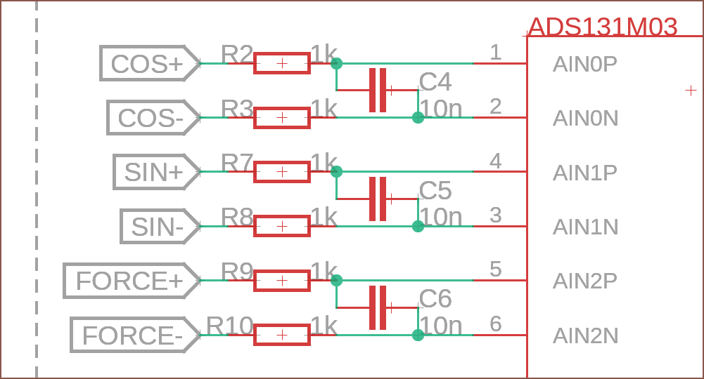
Looking back at that HX711 reference design, I remember that there were also resistors on the inputs of the reference ADS131M03 PCB. I've looked though the datasheet and it's actually mentioned right here:
That's a lot of passives, but ok... these are 0603s too...
-
[T] Eliminate interconnects?
06/20/2023 at 12:53 • 0 commentsI wasn't expeecting these to cost so much. Ther more I started researching into other options, the more I was wondering why I was bothering with both a cable that goes to Tetent and 2 cables that go to neighbouring Tetrinsics. It would be cheaper and neater to just have a higher-pin-count cable go out. This way, I could even put VBLDC on the FPC since it would just need to handle the current of one motor.
-
[L] DRV8311P Motor Controller Component
06/20/2023 at 12:46 • 0 commentsI thought I'd just get it over and done with regarding these new chips.
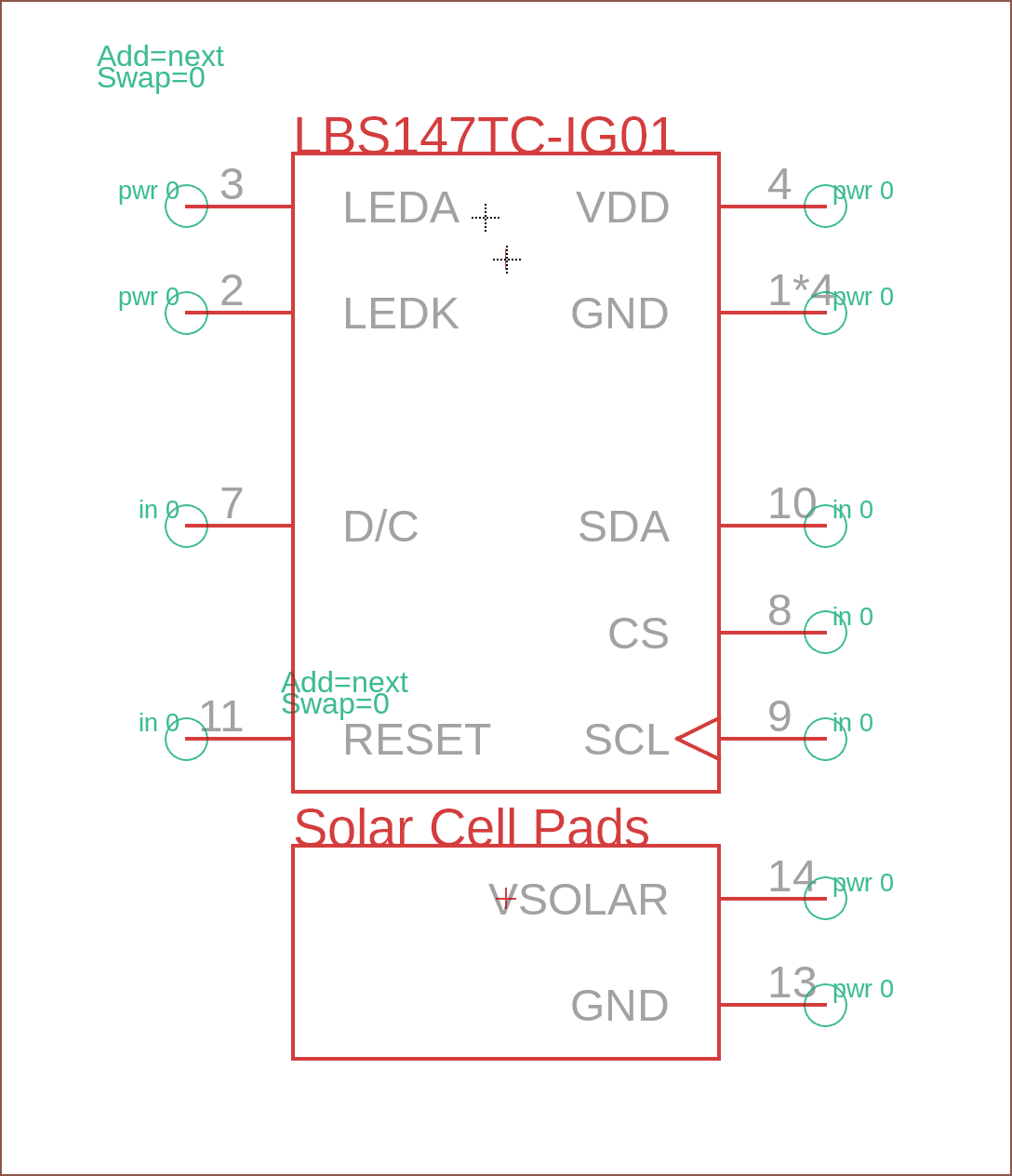
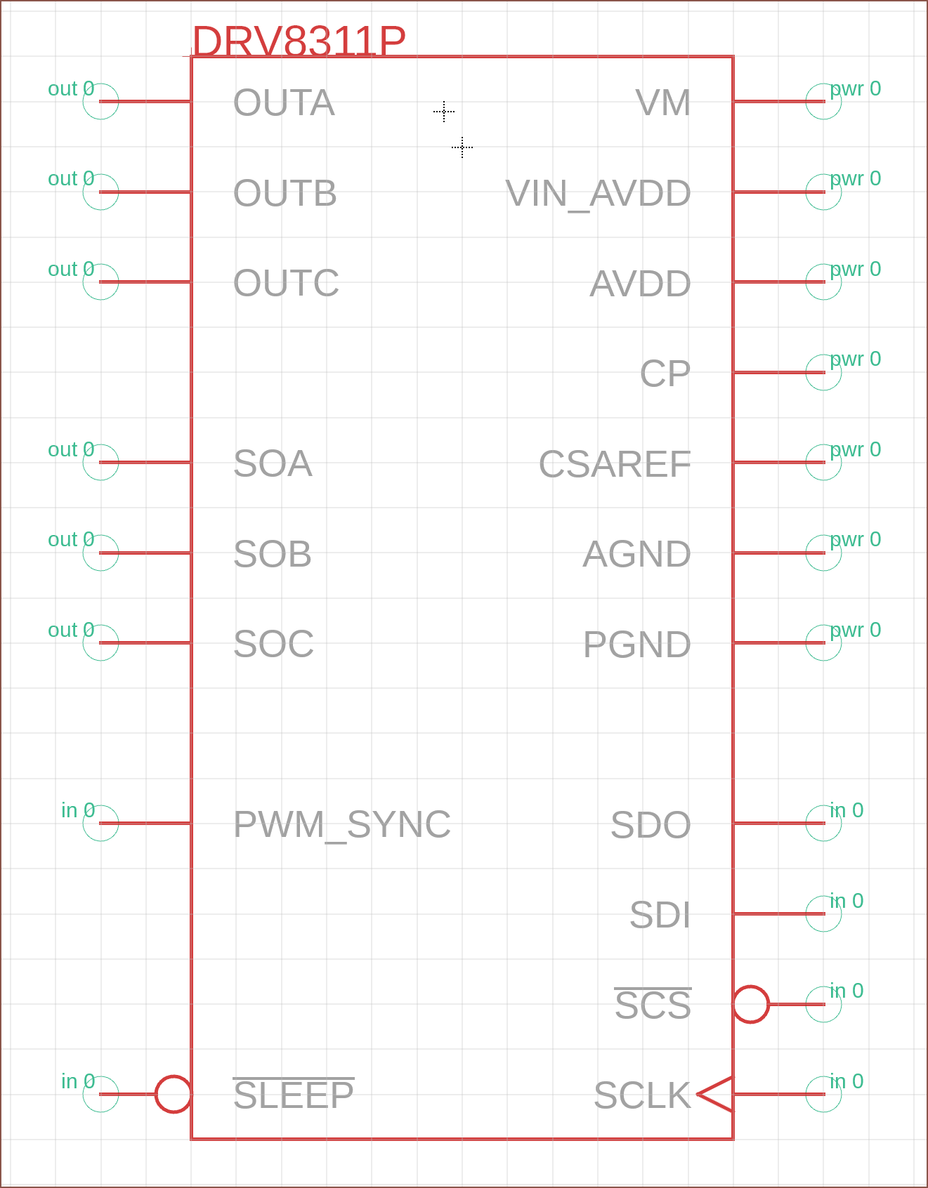
The symbol was straightforward:
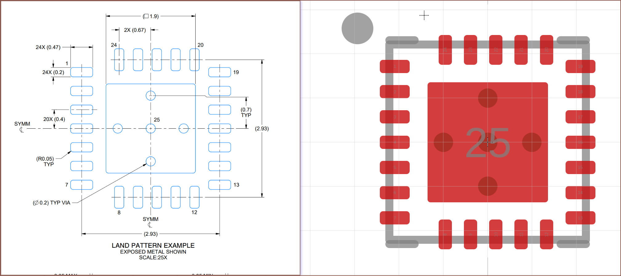
(I later add the missing pins) The pad though, totally isnt:
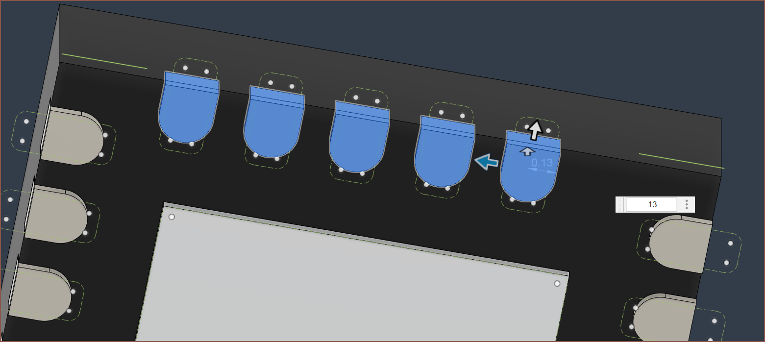
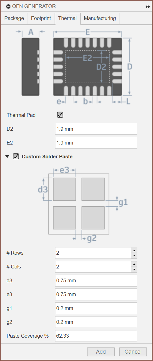
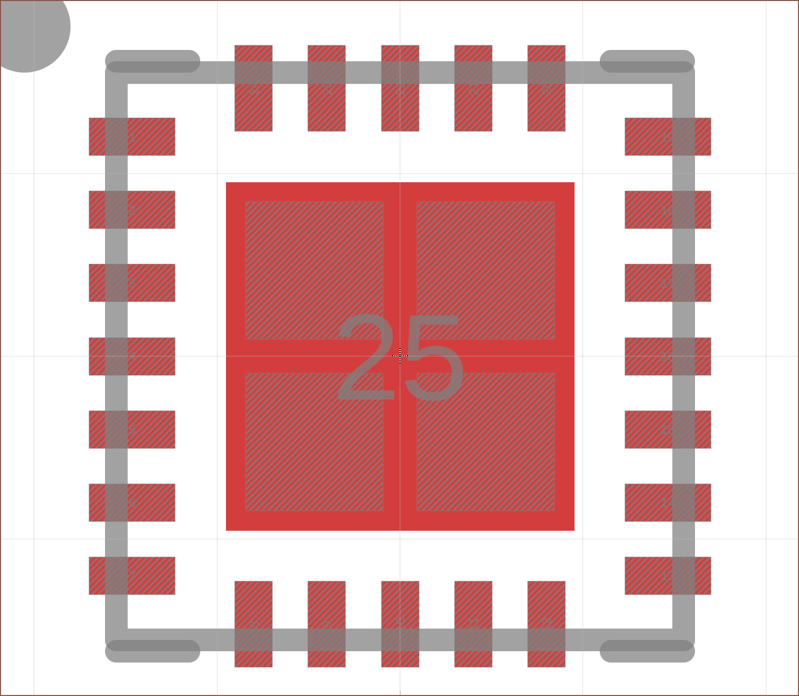
The top/bottom pads aren't centered and so I had to change the grid to [generated position] - 0.67mm. In this case, it was at 0.8mm so the grid was set to 0.13mm so that I could drag the pins. Then, I calculated the roundness percentage of the pins, which is 50% for everything other than the pad which is approx 5%. Lastly, I changed the grid to 0.35mm so that I could spawn circles which I put on the via layer. I looked at JLCPCB ahead of time, and it seems that there are multiple min-via sizes and I'd assume that the other ones cost more.
Unlike how Fusion 360 is usually nicely parametric, I have to manually move these pins over even though the footprint would be updated automatically. It's also a shame that there's no way to specify rectangular pins along with your rectangular pads.
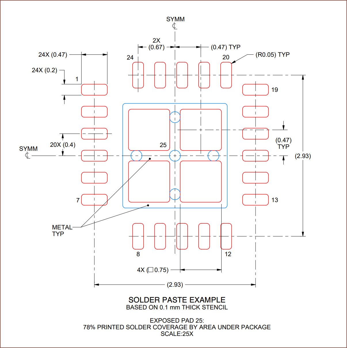
So I do all that, and then I scroll to the next page:
There was this window that I walk passed and skipped. Now this wouldn't actually be an issue if Fusion 360 actually reverse-synced the package to the footprint, but it doesn't. So I'm now doing this all over again to get the correct tCream so that I can copy-paste it.
Not sure why Fusion 360 Electronics likes to throw me under the bus when it comes to footprint creation. It just seems unpolished with a hint of legacy design architecture.
-
[R] Are better components now available?
06/19/2023 at 20:48 • 0 comments[20 June: 01:00]
So I stopped daydreaming about the T9 Plus mini PC inside #Leti and went onto Digikey to confirm prices of components. Unexpectedly, prices have changed.
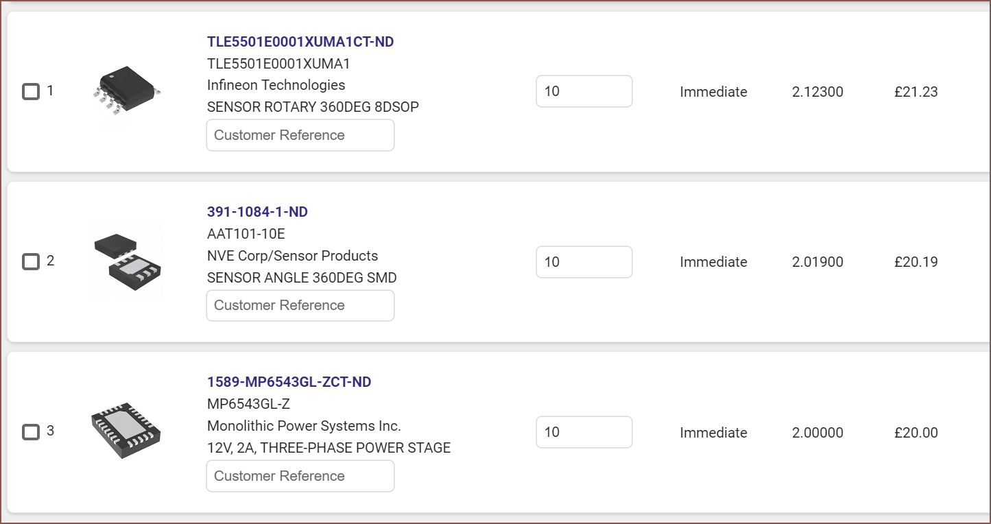
The TLE5501 was over £3 last time I checked, and the AAT101 was in the £5 range IIRC. Looking in my spreadsheet I haven't updated since March, I can also say that the MP6543 is also a tad cheaper.
What does this mean? It implies that components that the semiconductor price hike is on its way out, and there could be components on Digikey now that I wouldn't've considered months ago. I'm making this log realtime to see what my options are.
Motor Controller
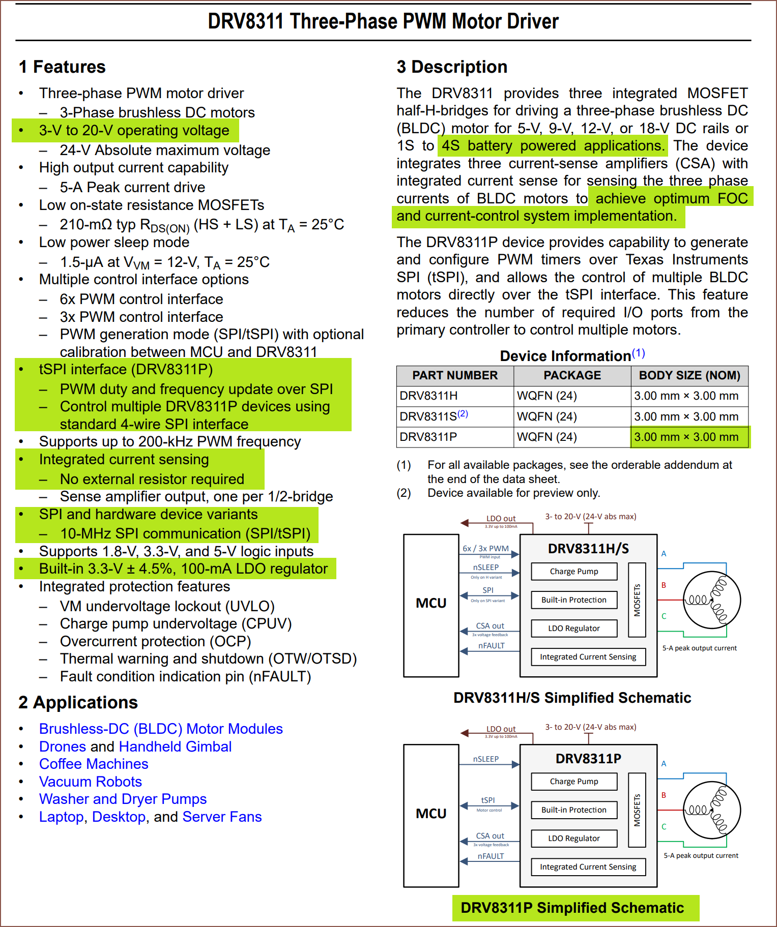
The first thing to catch my eye was this DRV8311P. I momentarily saw the TMC6140-LA before this but I didn't like the idea of having to bring my own MOSFETs. This chip though? Well...
- It's cheaper
- It's smaller
- It's got a wider working voltage
- potentially allowing for direct 4S Lipo power (as planned for in #Leti) if the 580KV motor allows for it, which is unlikely considering what's said on the listing:
It is a miniature three-phase brushless motor without Hall,
aluminum alloy shell, rare earth medium-strength magnet,
double ball bearing.

We use the ESC of the model aircraft to drive the motor,
the maximum speed is close to 7000 rpm at DC12V, and the
KV value is about 580. It is estimated that as a gimbal
motor, its speed should not be so high, and its rated
voltage should be lower than 12V. Motor weight: 10 grams
Test voltage: DC12V (driven by the ESC of the aircraft
model) No-load speed: 7000 RPM The motor works beautifully,
runs silently, and the torque at DC12V is also OK
- potentially allowing for direct 4S Lipo power (as planned for in #Leti) if the 580KV motor allows for it, which is unlikely considering what's said on the listing:
- It uses SPI, saving 6 PWM pins and meaning that I can remove the 74HC595 from the equation and still have a pin spare.
- It has a slightly low MOSFET resistance?
- 210mOhms vs 2 x 110mOhms = 220mOhms on the MP6543 for the
- I don't have to bring my own current sensing resistors.
- That would've been a real help when I was designing the first PCB!
- It still has the LDO source, but it seems closer to 3.3V
- MP6543 is "typ. 3.45V".
Ok, I'm changing to this. Shame I spent £5 on an MP6543 chip for the prototype that I'll now never get to use (like so many other components for other projects).
Angle Sensor
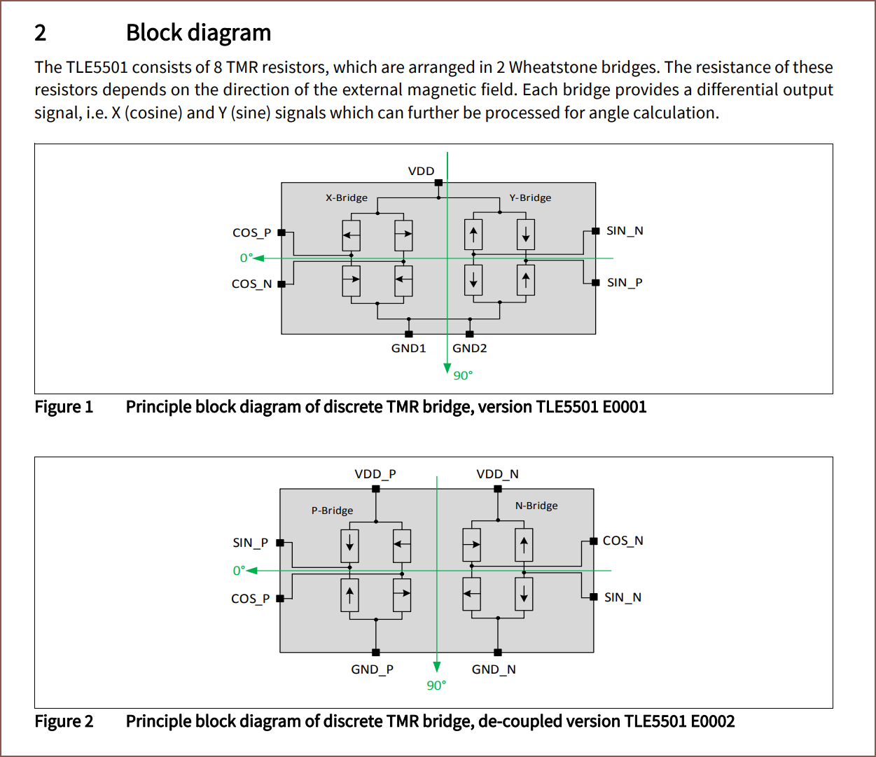
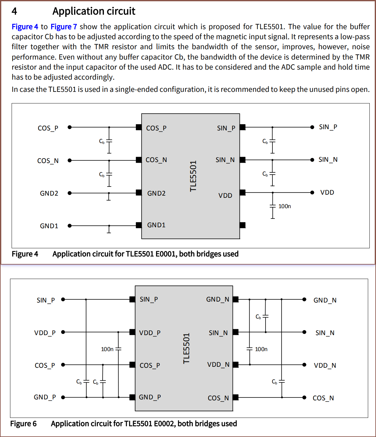
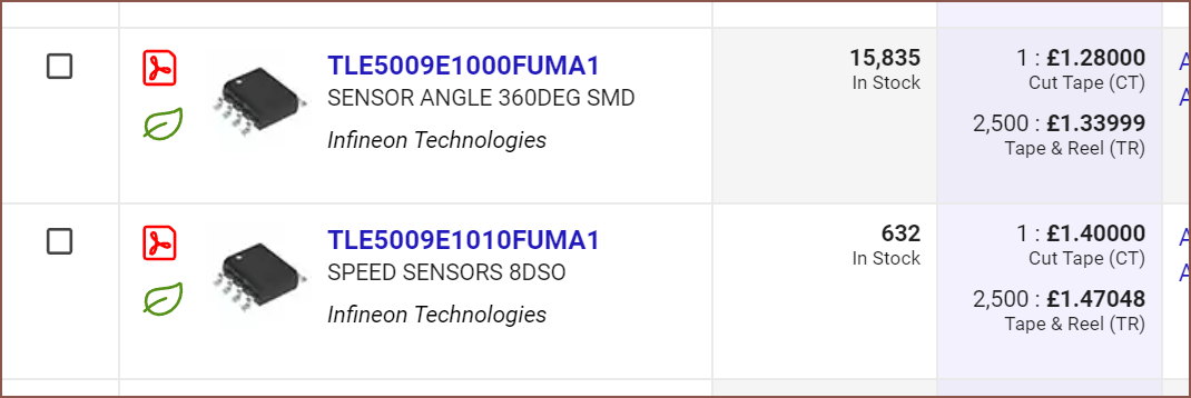
Turns out that the below is the difference between the one already in my basket and this one above:
Unlike the E0001 that seems straightforward to understand, I'm not really sure how you're supposed to connect all these VDDs and GNDs to the rest of the circuit. At least I know that the capacitors for this are supposed to go to ground and not to each other, like what I have in the schematic. They're, once again, optional, so I'm just going to remove them entirely.
The next cheapest chip is the TLK5009 E10X0, which seems to have been made 6 years prior.
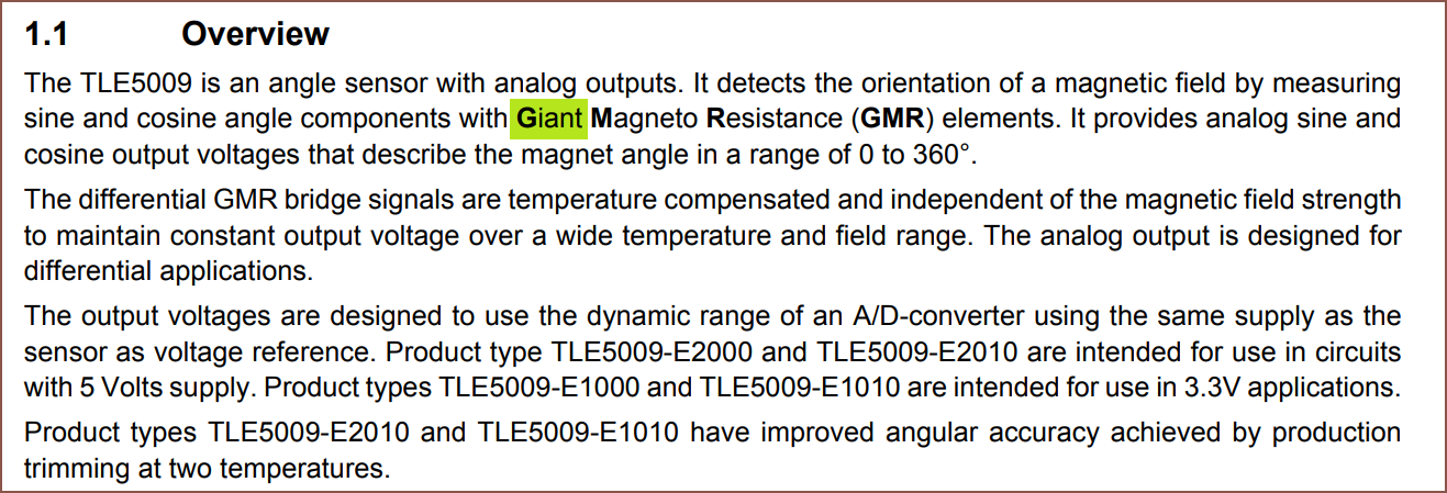
I'd assume spending the extra 9p (MOQ 10pcs) for higher angular accuracy is beneficial for a prototype. So far, I can only tell that GMR has a much larger wikipedia page than TMR, there's a 5th ADC pin for a temperature porportional voltage with the GMR IC and that the TMR IC has a larger magnet range of 20 - 100 mT as opposed to 24 - 50.
I tweaked my search parameters and there's another one. It seems that it's a wheatstone bridge that then goes into an amplifier to produce 2 output voltages, which could allow me to go down to a 4-input ADC. It's specifically designed for BLDC applications, which is a good indicator that I'm looking at a potential option here.
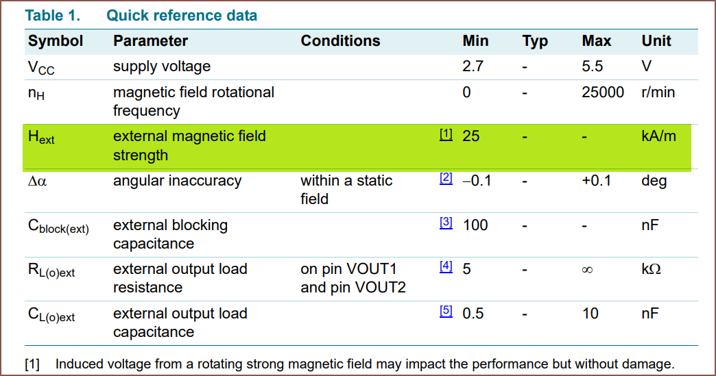
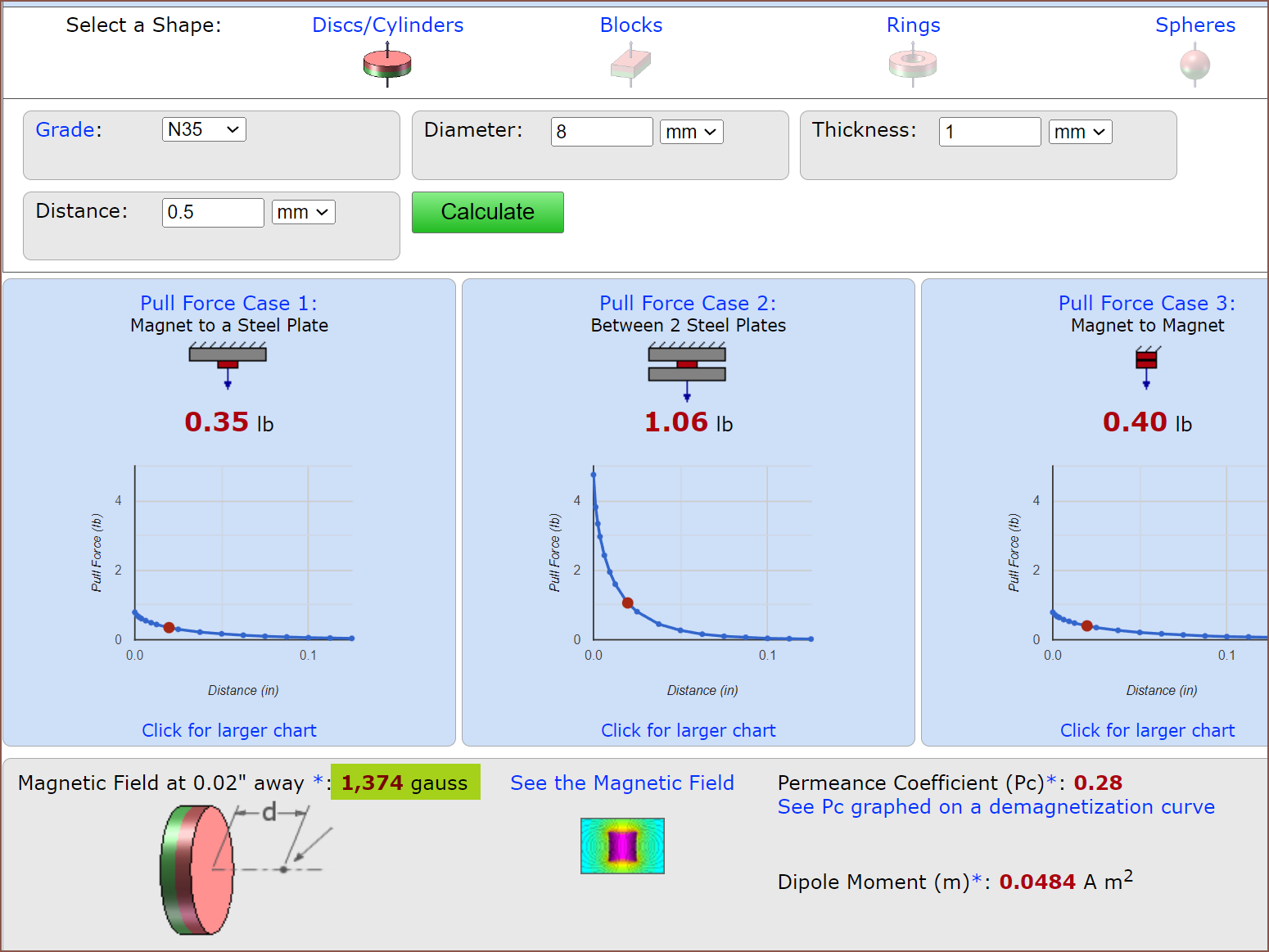
The most notable thing is that, unlike the other chips I've seen is that this doesn't have a maximum field strength, and the minimum is 31.35mT (converted). For the AAT101, there also isn't a limit and instead specifies a required magnetic field strength of 3 - 20mT (converted). The values were denoted in Oe, and 30 - 200Oe looked like the min-max up until now, when I'm looking closer into all these datasheets to compare this shortlist. There isn't a diametric magnet uption, but hopefully the settings I've put in are close enough to work from:
Throwing that into a converter, that's 137mT. If I go for a wider gap, I could get into the 5501's extended range:
The KMZ60 seems to offer better accuracy too, coming in at +/- 0.1 degrees instead of the +/-0.6 degrees for the TLE5009 and +/- 0.5 degrees for the AAT101.
There's an output pin similar to the 5009, but it seems to be optional. There's also an input pin that sets up the internal temperature compensation.
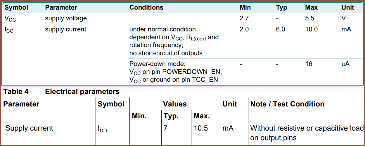
The power consumption of the Z60 is 6mA, which I thought was high (remember, there's 8 of these per Tetent) but at least could be turned off. Turns out the 5009 uses more power and doesn't have such an ability to be turned off. This is all in contrast to the AAT101:
AAT-Series sensors are resistive devices with no active components,
so they have no minimum voltage and can be powered from single
cells. With their low power, the sensors are well-suited for
operation from batteries or harvested power, and can run
continuously for many years on small alkaline, silver oxide, or
lithium button cells.
I've wrongly assumed that this non-active-component thing was the case for all magnetoresistive chips. It was all going good until I found this out. I never included the TLE5501 in the calculations for Tetent Taic, but at least it has a lower power consumption of typically 1.67mA and max 2.5mA.
The 5009 is unsuitable for this application, and the 5501 is on thin ice since I'm trying to get a solar powered edition. Wait... the AAT101 is cheaper than the 5501 E0001 now, and the only reason I was considering it was because it might be easier to install on a PCB (and the E0002 is cheaper if I can figure out how it's implemented into the current design). Considering all the other QFN's in this project, I don't think one more would increase the difficulty. Additionally, it's possible that I could have the chip and ADC on the same daughterboard, reducing the distance between the sensor and the sensing device and (ideally) reducing noise in the process. That idea might not work for these larger packages.
I'm not eliminating the Z60 just yet, because I want to look into one more thing...
24 Bit ADC
Mmn. Couldn't find anything cheaper.
Angle Sensor Conclusion
Since I can't find a cheaper compatible ADC, I think the power and space savings of the AAT101 are more important than the 5X higher precision of the KMZ60.
PCB
Thinking about it, there's actually not that many components, traces or passives now, so perhaps I should try making a PCB where the ESP32-S3-MINI mounts on the bottom and all the other components on the top:
The FFC cables might get interesting, but this method is more versaite for projects that aren't specifically Tetrinsic.
Changes to Implement
- MP6543 ➡ DRV8311P
- 74HC595 eliminated
- TLE5501E001 ➡ AAT101
- Side PCB schematic ➡ Under-Motor PCB schematic
Log creation time taken: 5 hours, 24 minutes.
-
[T] Looking ahead: USB Type-C system
06/18/2023 at 22:08 • 0 commentsRight now I'm just looking further ahead at the Tetent implementation to see if there's anything else that would be required to connect to a Tetrinsic that can't go though I2C.
- Essentially, the part that'll likely be called Tetent PCB is a PCB that has
- 2 USB Type-C ports,
- maybe the DAC if there isn't enough space to use the off-the-shelf stuff,
- the USB PD chip that negotiates (ideally) 12V,
- This is because both the BLDC, BLDC controller and any potential mini PC I use in #Leti use 12V. I wouldn't be suprised if the DAC and speaker also worked on 12V.
- and the circuit that deals with charging the batteries.
- I could probably get that one seller to put together a 2-cell for Tetent, but I'm also looking ahead at #Leti and how I'd (ideally) want 8x 5Ah cells. That's 148Wh, and airlines accept up to 160Wh in carry-on, though I've only seen references for power banks / spare batteries. I certainly don't fly often enough to worry about it right now though.
So far, I've found
- Essentially, the part that'll likely be called Tetent PCB is a PCB that has
-
[L] Expansion Pins
06/18/2023 at 06:26 • 0 commentsSo I've looked into the TC358870XBG and it seems that 2 I2C pins, 1 reset pin, 1 clock pin and an INT pin is needed. One probably could make a circuit that generated the clock instead of the MCU, but a free pin is cheaper than that.
The main issue I was having was the INT pin, since it seems that it acts as a strapping pin (as in it sets the I2C address on reset) and an interrupt pin. I didn't have the 3 - 4 spare pins for interrupts, and I was thinking of seeing if I could connect the BLDC controller to a 3:8 decoder to free up some pins, but then I remembered that a single Tetrinsic doesn't have to control it all. Thus, instead of each Tetrinsic having (or trying to have) a
- MIPI_RESET
- MIPI_INT[0-3]
- CLK_MIPI
- ADDRESSABLE_RGB
- DAC_SD
I can have 2 Tetrinsics focus on 2 of the pins. As long as 4 Tetrinsics support all the features, it's ok.
-
[L] BMI160 3D package and 74HC595 output extension
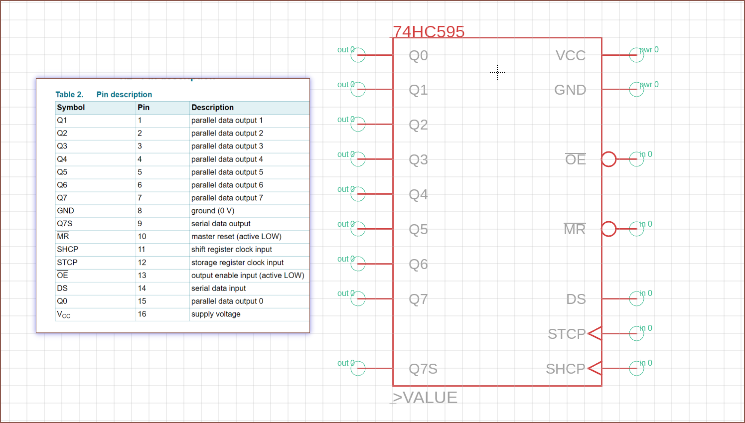
06/16/2023 at 19:48 • 0 comments[Here] is the chip I'm using. Below is the symbol I just made:
Now to make the footprint and 3D model...
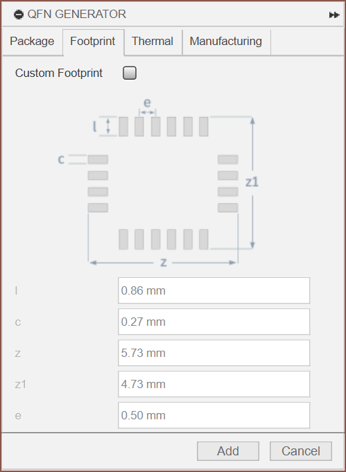
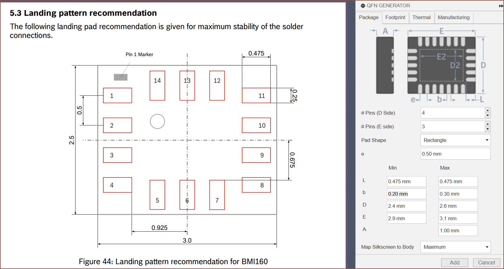
Hmm? I wonder if I could've used this to create the BMI160 footprint...
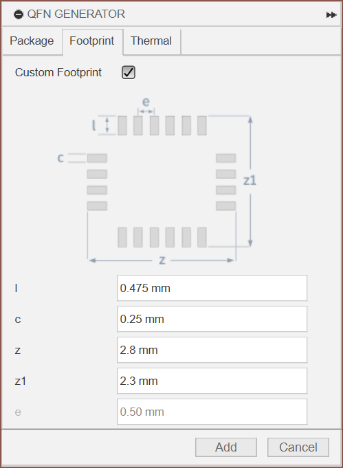
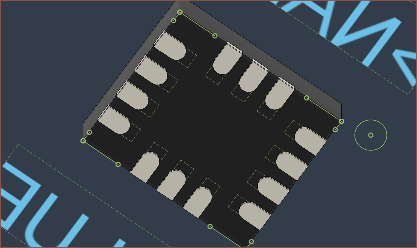
The 3D pads are understandably wrong, but it looks like there's promise with the footprint.
It's actually just as I manually modelled. Amazing.
It's just a shame that I have to click each pad line individually when projecting it. For some reason I couldn't just click+drag to select all. To save time, I just projected half and circular patterened the other half.
Anyway, back to what I was supposed to be doing... connect these pins... join these lines... done.
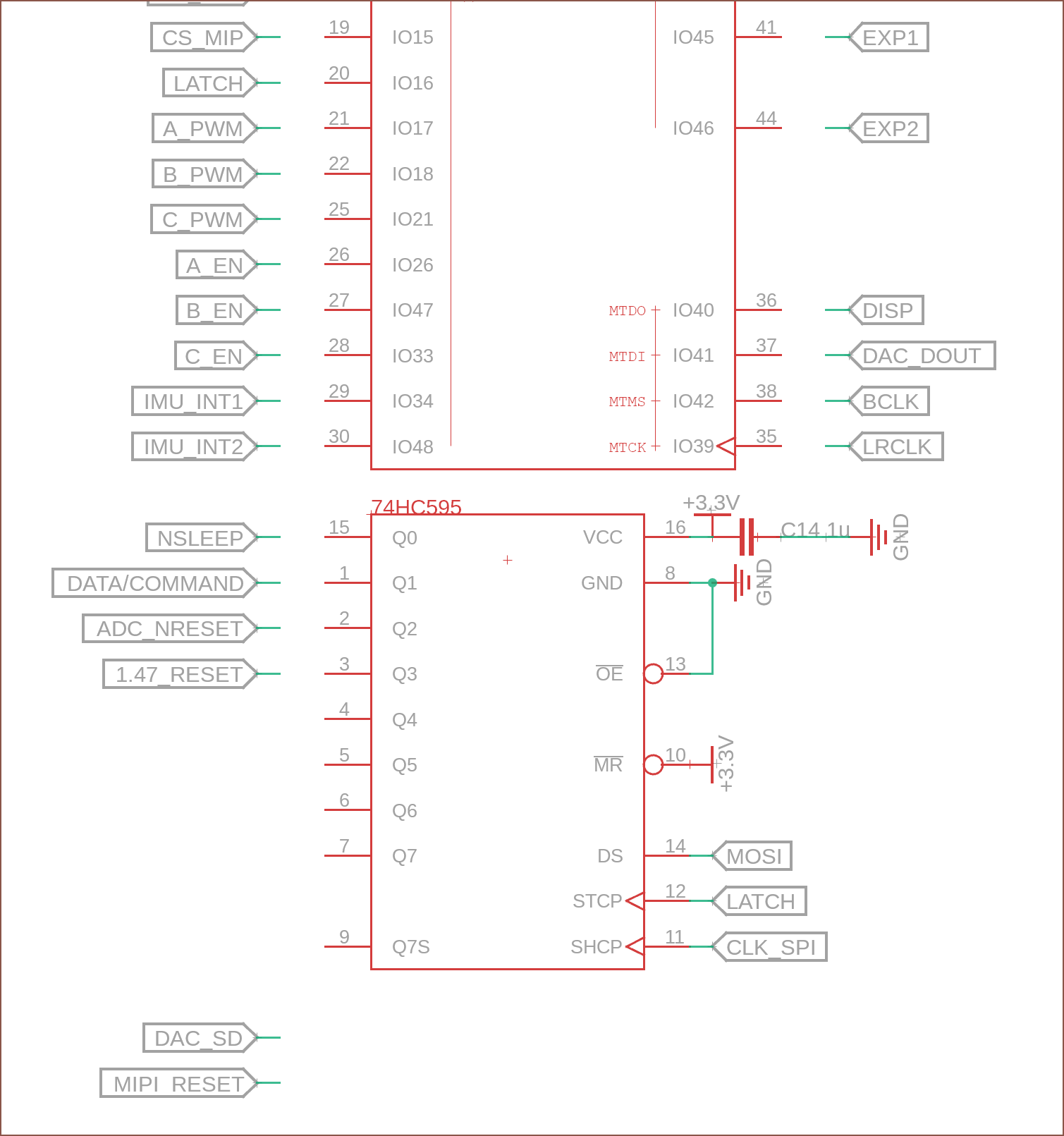
Talk about Team Close (TM). Thankfully, I can populate half the 595 with the pins that just power down or reset other components, meaning that they're very unlikely to need to be changed often. There is then 1 free pin I can use for the latch. I should be fine with nSleep and DAC_SD, but I'll have to check to make sure that the 1.47" LCD and ADC don't expect to be communicating at the time of the reset pin.
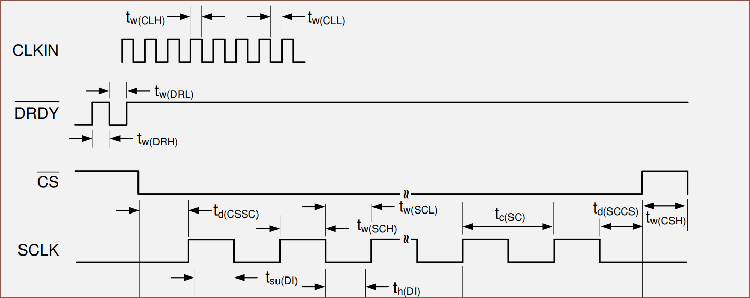
For the ADC, it seems that as long as it has an actual clock source (and I don't try and share the ADC clock with the SPI clock like I proposed doing in the past) I should be fine here. Actually, looking at the diagram just above it in the datasheet, it looks like the SPI clock isn't even on all the time:
I wouldn't be able to share the 2 sources anyway, since the MIP display expects maximum 2Mhz SPI clock and the ADC uses 8.192Mhz for it's CLKIN.
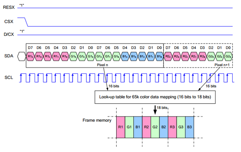
On the LCD side, it actually looks like I could even put D/C on the 595 if I needed to, since it's just a toggle between telling the display if you are sending either data or a command. I can't imagine you'd need to rapid toggle for that. Still though, the less pins are on the 595, the faster it is to update all of them.
Me about a week ago was worried that "How am I going to get Tetent done by the end of summer at this rate?", but wow now I've almost finished the primordal schematic! I've now got to- do the power circuitry of the ESP32 (if I need more than just a bypass capacitor),
- create pads for the load cell and magnetometer,
- create the potentiometer for position selection,
- expose the USB pins (and UART if I need those for programming),
- add test pad connections,
- remove the grounds in the Tetrinsic_PCB connector,
- It's probably better to go with either another 3V3 or another pin
- and look into the TB chip connections.
- It's likely that it too will have some non-I2C pin that needs to be connected to the MCU.
-
[L] MIP LCD and Not Enough Pins
06/16/2023 at 17:33 • 0 commentsSo I started looking into the 595 IC once again, but it doesn't seem that I'd be able to send a PWM signal though it all that well. I decided to instead look into implementing the last thing (that I can remember, at least) which is the Memory In Pixel LCD from JDI.
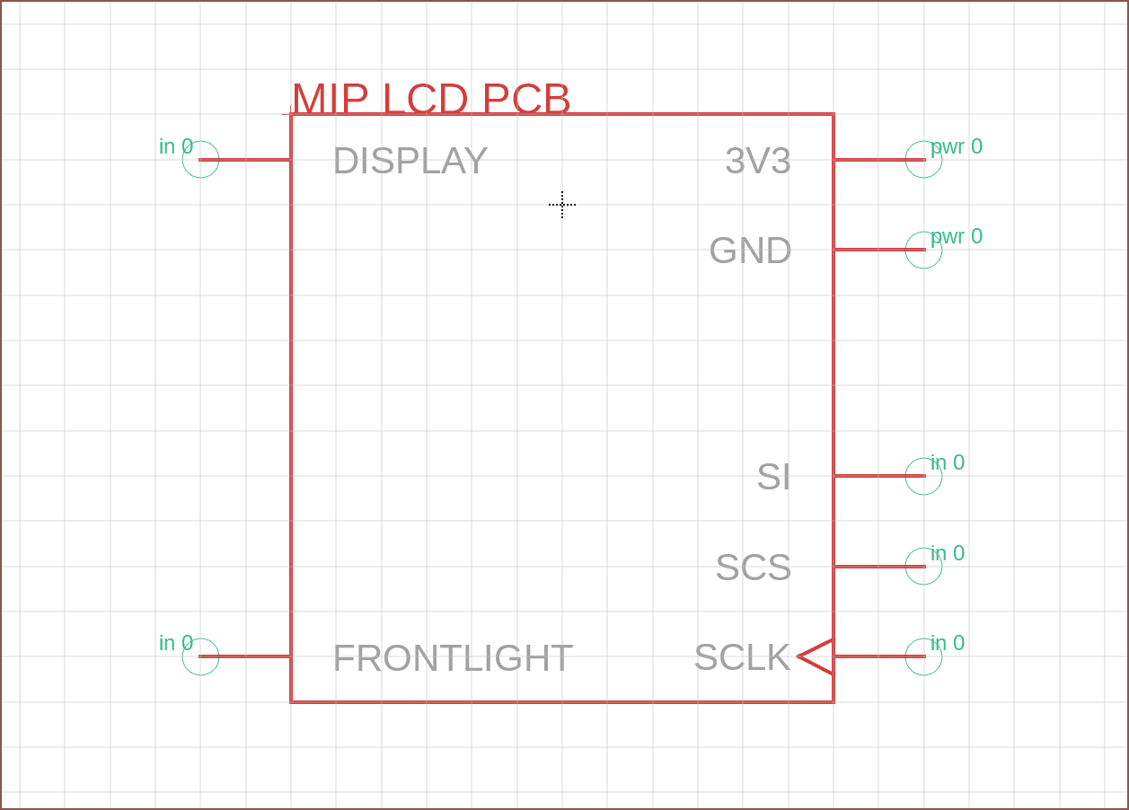
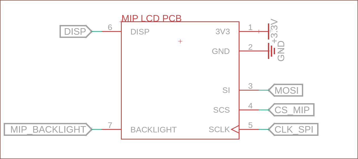
I was able to find this project which also includes the schematic for a breakout board. From the readme, I've created a symbol of the pins that I'd need to actually controll the board, and will put all the other components on a small PCB behind the display itself. Since I'd like to see if I can use a single 12P ribbon cable for all interconnects, an idea I've got is to also have the addressable RGB also connect via this LCD daughterboard (instead of having to make pad space on the main PCB). I'll see if that's a good strategy at a later time. For now though:
In the schematic, it looks like this:
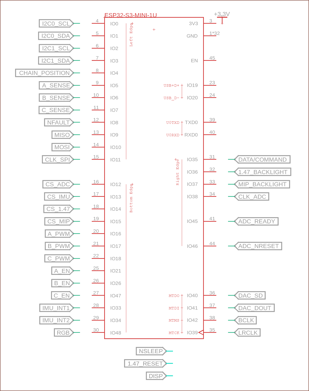
And that should be the last main component, so my pin utilisation looks like this:
CHAIN_POSITION is a new addition which aims to use a potentiometer to set what position in the chain the Tetrinsic believes it's in. Ouch... over by 3 pins. Ok... looks like I'm going to look into that 595 chip and see if I can get out of this.
Tetrinsic [gd0041]
A motorised fader that is continuous, pressure sensitive, haptic and water resistant.
 kelvinA







 Unlike how Fusion 360 is usually nicely parametric, I have to manually move these pins over even though the footprint would be updated automatically. It's also a shame that there's no way to specify rectangular pins along with your rectangular pads.





 There's an output pin similar to the 5009, but it seems to be optional. There's also an input pin that sets up the internal temperature compensation.