-
[E1][L] Tetrinsic Pad
06/16/2023 at 02:29 • 0 comments[L] = [EM] = Electronic design
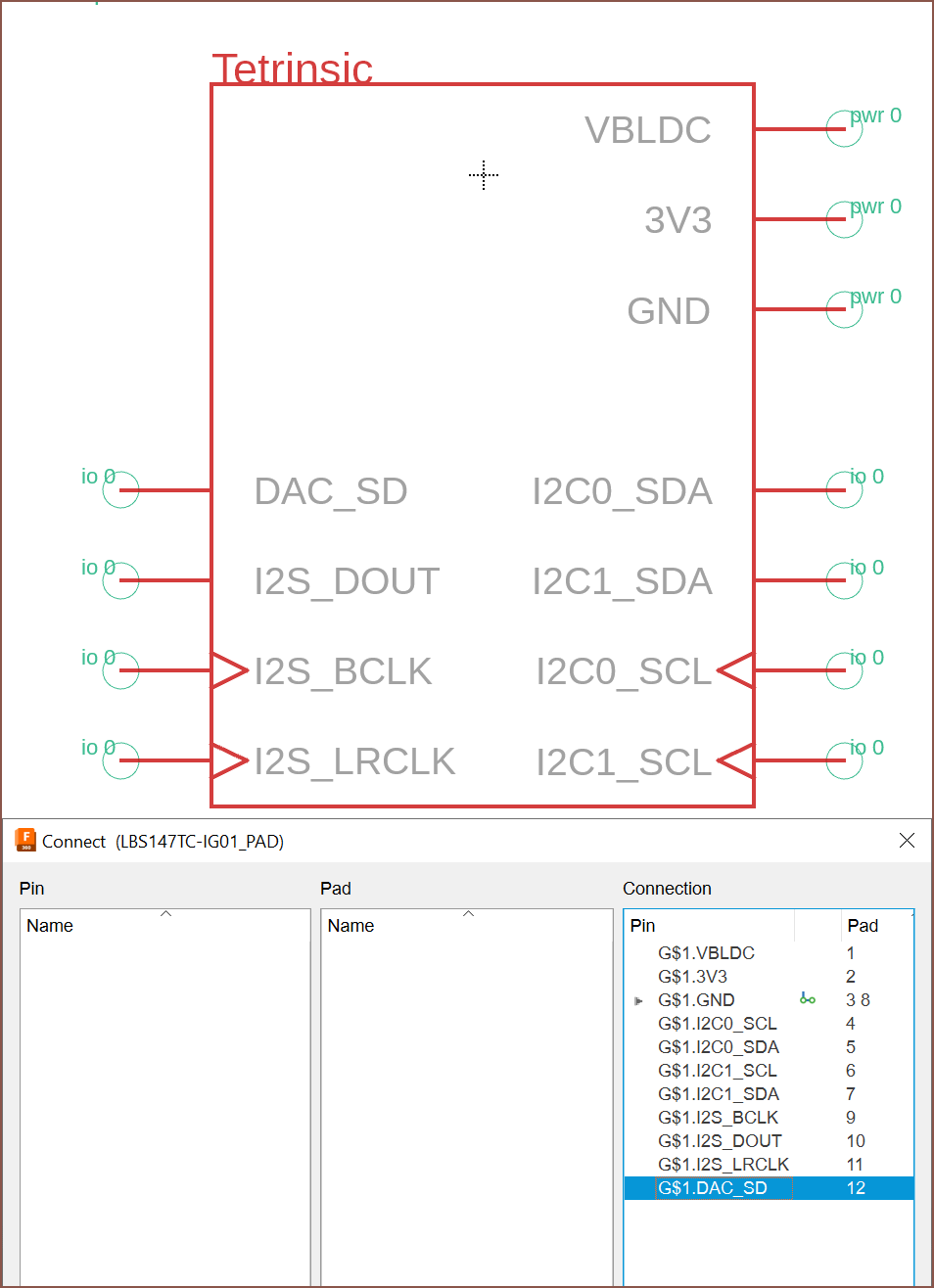
So I've found out what I need to do to connect the off-board MAX98357 via I2S and I've got an idea to use the same type of ribbon cable (and pad) as the 1.47" LCD:
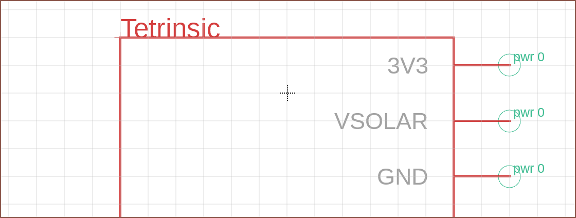
I've used the GND pins to split the power, I2C and I2S sections apart.
Now thinking about it, I probably shouldn't power the BLDC through the ribbon cable because there's another 7 it also would have to power. I also need an addressable RGB pin.
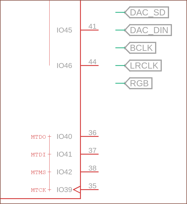
All these additional pins means that I'm seemingly out. I wonder if I could actually use those bottom 4 IOs.
It totally sounds like I can. Even then, I've got 1 pin left and 1 memory LCD to connect. I'm going to need to parallel-out some pins.
[Edit 1] I just remembered that, for Tetrinsic Taic, I need the photovoltaic cells connected in parallel.
-
[EM] 580KV Motor Pad
06/14/2023 at 22:20 • 0 commentsBefore looking into the I2S implementation, I'm thinking that I'm getting more confident in creating electronic library components now and should actually make the BLDC motor pad instead of mentally remembering its existance.
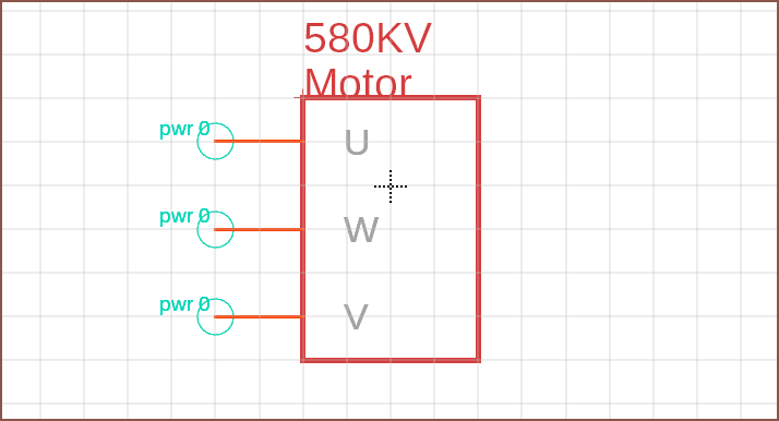
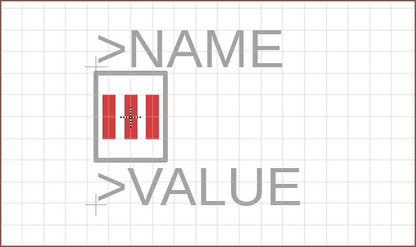
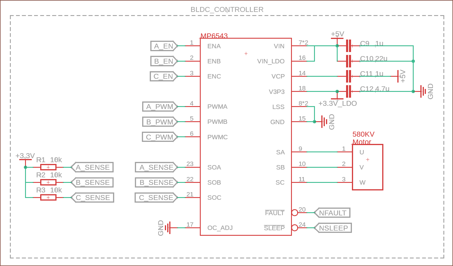
Not sure if the pins should be marked as "in" or "pwr". I'm going with "pwr" for now. It's plainer than the one I've designed in EasyEDA, but it doesn't matter. I can come back to this at a later time if needed. I've gone for 0.6 * 2mm pads. The spacing of the FFC is 1mm. And there we have it. I've also added values to the 3 sense resistors. Also, I'm not sure why the order was "U, W, V" in the EasyEDA schematic and not "U, V, W". I'll also have to check if 10K resistors are fine or if I should lower them to 4.7K.
-
[EM] LBS147TC-IG01 (1.47" LCD) Pad
06/14/2023 at 21:53 • 0 commentsThe component
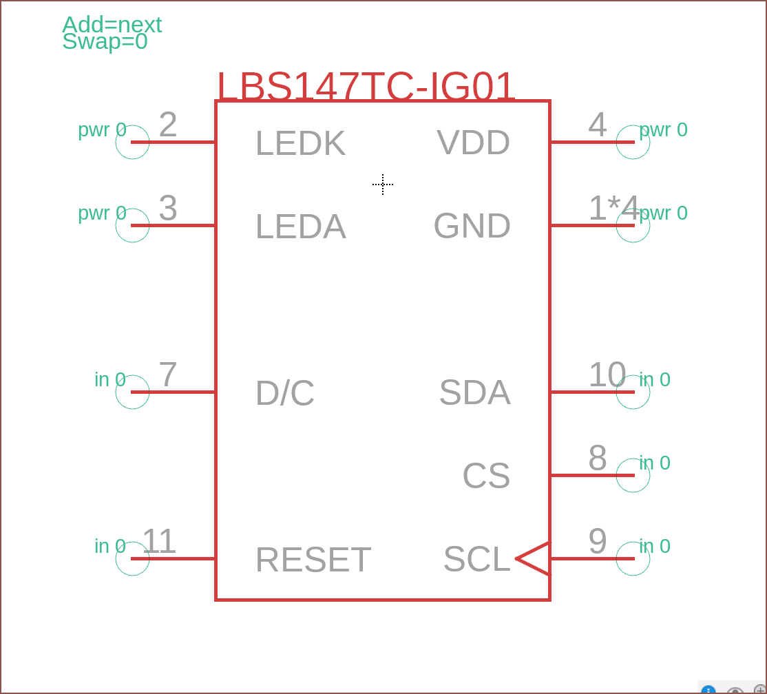
I want to see ASAP if I'm out of pins. I was going to just line up some pins someplace in the schematic to show "this is where a pad goes, but I don't know the fine details of it just yet". However, I was stuck like a frozen loading bar and decided (after taking a little browse to see what my other ECAD options were) to just make an actual component for the thing:
The cool thing is that there are 2 open source PCB schematic designs for this screen, from waveshare and dfrobot.
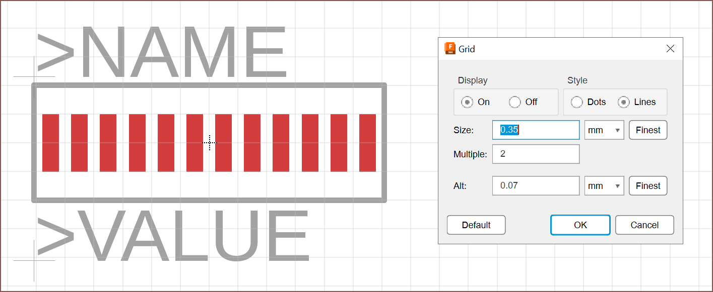
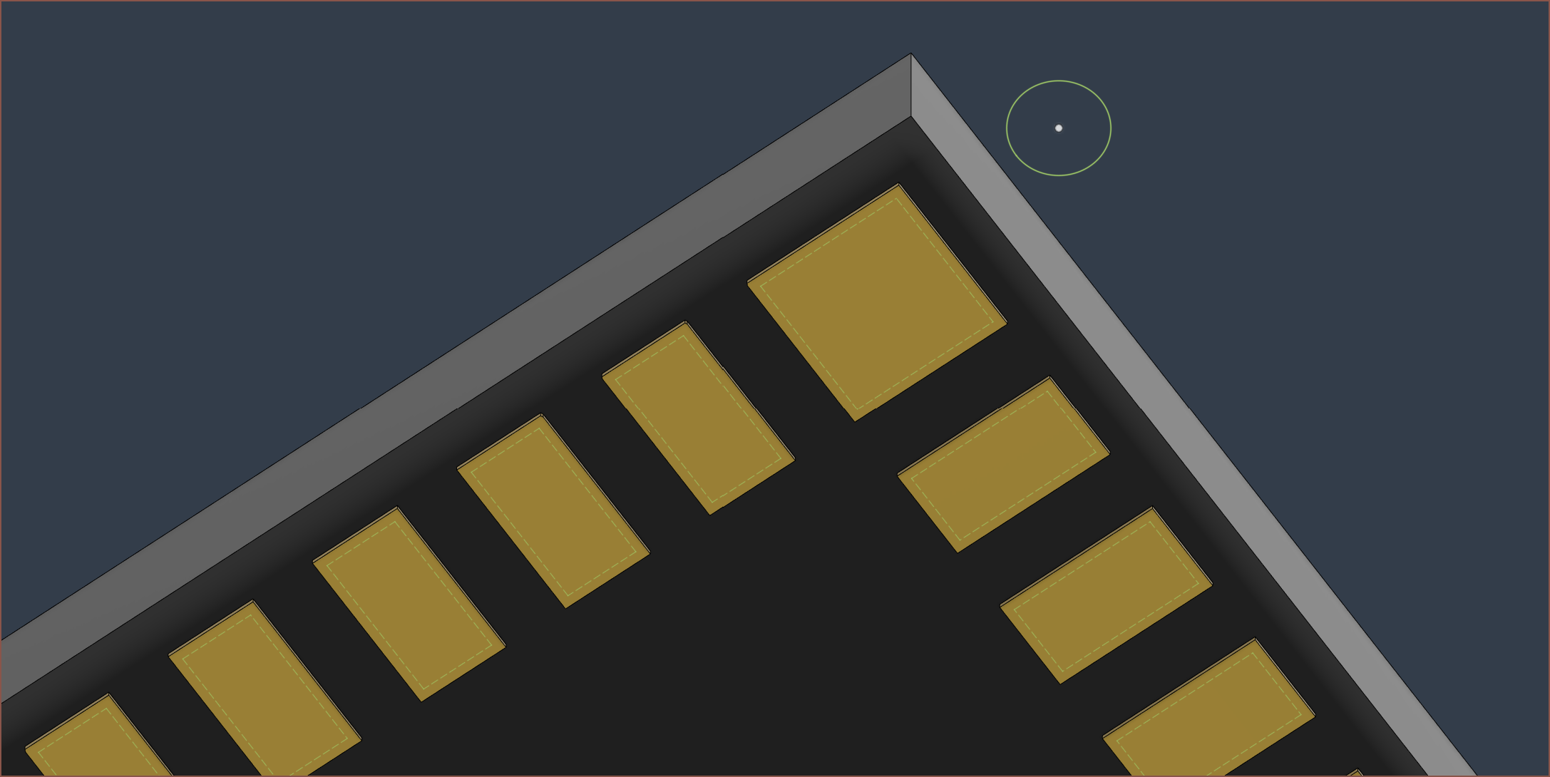
Back to talking about Fusion 360, I found out a couple things. First, I can change the theme in Preferences, and I changed the PCB/footprint editor to light (because I first changed the schematic editor to dark and it was harder to see), and the second thing I did was change the default grid to mm (since I'm mostly coming across mm specified pin layouts or it'll be something classic like 2.54mm anyway).For this LCD, the spacing is 0.7mm as claimed on the listing. Now, I thought I could just use the pin array and have my alts set to 0.35mm, but for some reason, after I click to place the pad, it nudges over to the nearest 0.7mm (which was my grid size when I tried it). Thus, I've come up with this better strategy which is to have half the grid size with "Multiple" set to 2.
Thankfully, this now means that creating this pad (and others similar to it) is super easy, barely an inconvinience, meaning that I don't have to worry too much about perfection straight out of the gate. I've used 1.4mm * 0.4mm pads currently, but this might increase to 2mm if the pads still seem like they'd be harder to solder.
Back to talking about the symbol, I've decided to keep things consistent with other components instead of doing the more traditional thing of listing out all 12 pins. Still, I haven't done any consistency tweaks like swapping LEDA and K around so that the +ve of the LEDs (LEDA) is inline with +ve of the pad itself (VDD). I'm also wondering if I should stay consistent and have the symbol be 12 squares wide instead of the 8 it currently is.
The circuit
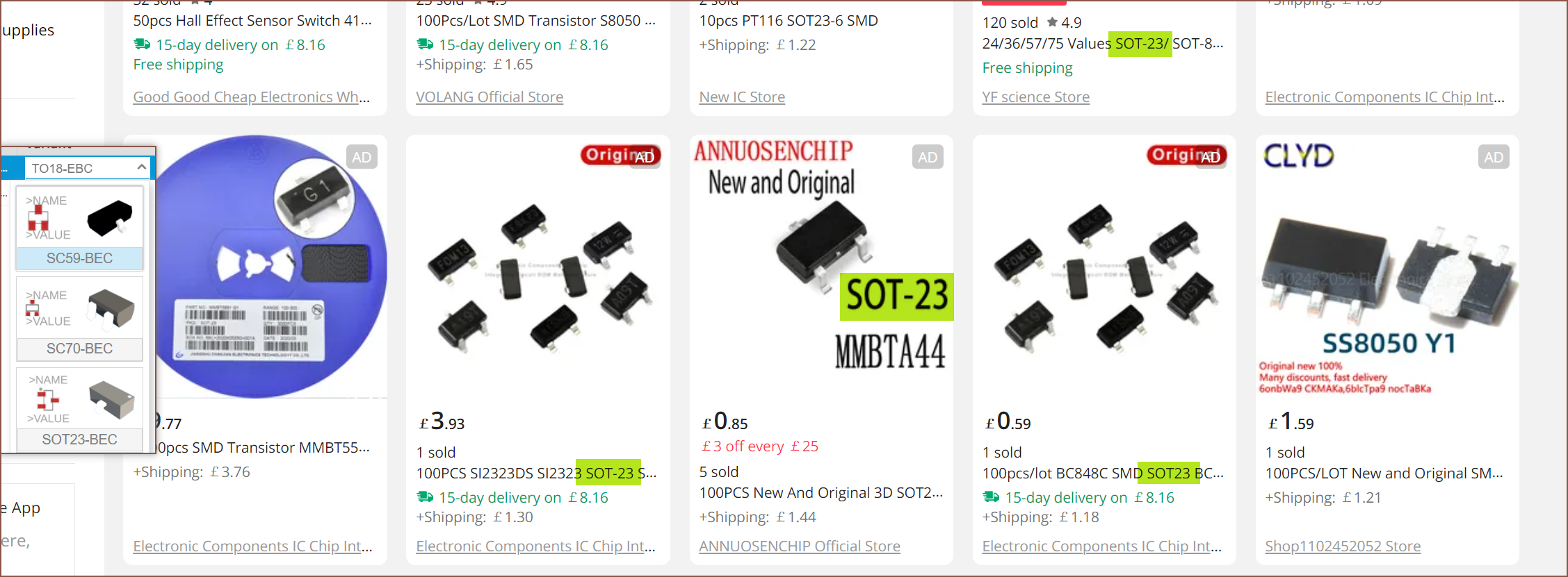
The backlight circuits in both PCB designs call for some NPN transistor. I looked at my options already available in Fusion360 and then searched "npn smd" in AliExpress. It seems that the SOT23 is the most common:
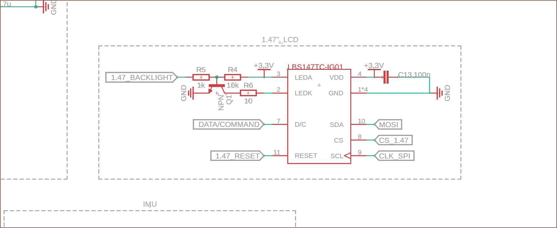
After that, it seems like it's just a quick slap together of components and pin names to get... this run:
This means that I'm another 4 pins down, and I haven't even looked into I2S yet. I doubt I could just send audio down through I2C so I better look into that next.
-
[EM] Pins and the GPIO Matrix
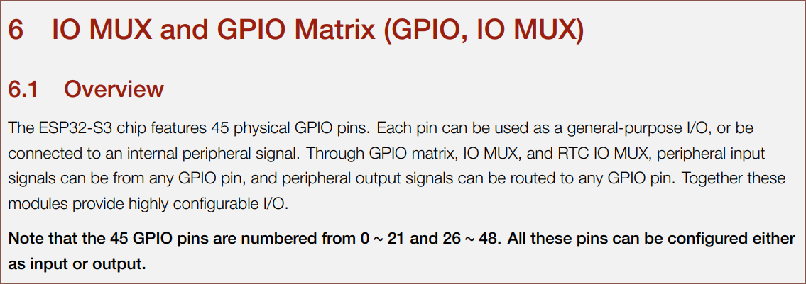
06/14/2023 at 01:15 • 0 commentsSo, as it turns out, the ESP32 supports the ability to route any GPIO to any physical IOx pin... at least... that's what I understand from trying to figure out the SPI pins.
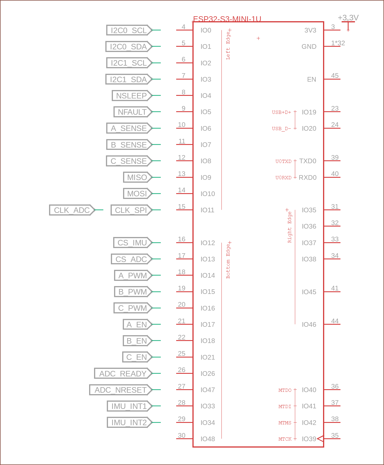
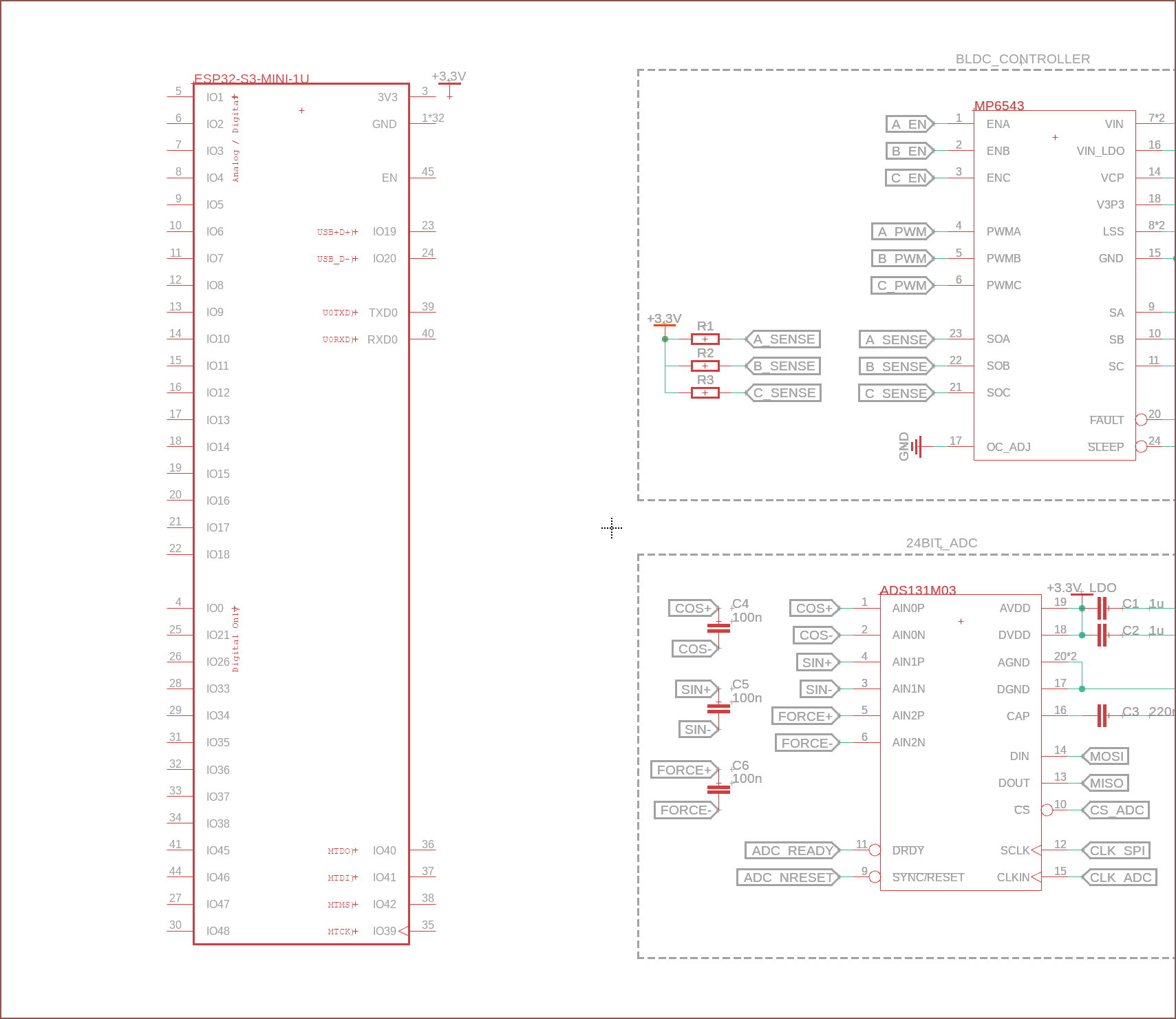
That means that my symbol is kind of lacking, and so I've revamped it:
As you can see, I've also started lining up the pins I need, and I only have 6 - 7 pins left for I2S (depending on if the ADC gets its own clock or not), 2 displays and an addressable RGB pin. The 8-bit shift register might make a comeback.
I've decided to expose both I2C channels for versatility (such as reducing traffic on an I2C bus), and to allow me to support communications with 4 Toshiba HDMI->MIPI chips for #Leti.
-
[EM] ESP32-S3-MINI-1U component
06/13/2023 at 22:40 • 0 commentsI think, other than the MCU, everything else connects to the PCB via some kind of pad array (a row of pins / pads). Thus, I finally tackled the ESP32 component. This also affected the components I've already made too.
This ordeal seemed more tedious than it really could be in this modern age of 2023, and so I've been imagining what I woud've done if I was making ECAD software (which I might need to look into further if the #SecSavr Suspense [gd0105] / #SecSavr Soapavr [gd0146] can actually fabricate PCBs). Why can't we snip bits of the PDF diagram into some kind of OCR? I've only seen black + white diagrams, so it sounds straightforward (though I know that's usually never the case).
I'd like to mention that part of the reason I actually got through all of this is because of this Aural Scan sound generator I found. It sounds like cinematic background music of a personal technology lab (depending on the preset).
Symbol Formatting
Almost immediately, I thought it was going to be excessive listing every single feature each pin does. Even when I did that for the BMI160, I just used the datasheet anyway.
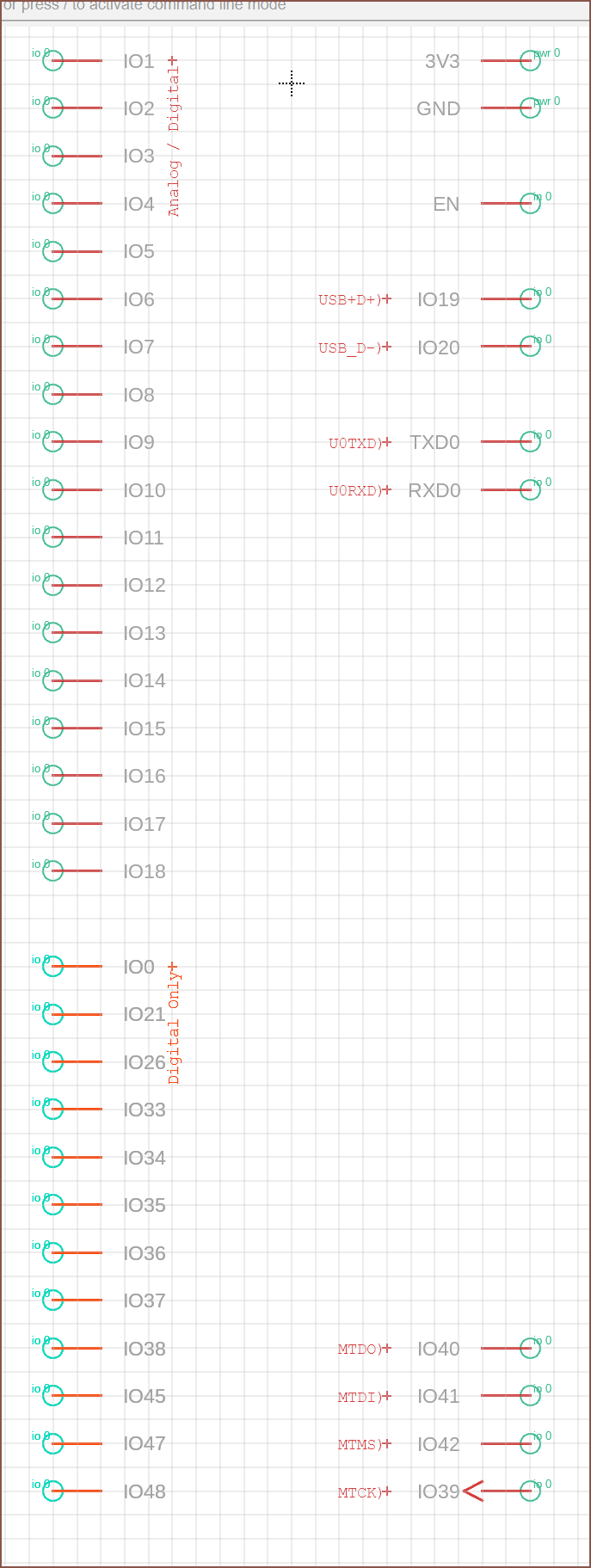
The first thing I did was try only putting the pin function I'm actually going to use in the pin name. Then I got the idea to actually take it out of the pin name entirely and instead make it a bit of text.
It was a good idea too, since it seems that changing actual pin names could spell trouble.
For some reason, those little '+' things next to the text don't show up in the preview but DO show up in the actual schematic. If anything, it should've been the other way around IMO. I decided to change the font of the text to "fixed" instead of "porportional" as the font was thinner and it allows multiple pin definitions to still line up correctly.
I then discovered thad adding '!' puts a line above the text in the pin name (and another stops it). Thus, I've changed all the nPIN_NAME's into !PIN_NAME.
At the moment, there's not much I could really group the GPIO pins into, so I just split them into Analog/Digital and Digital Only. This does make the symbol rather tall, but it's still tidy and compliant with the other symbols.
3D Model
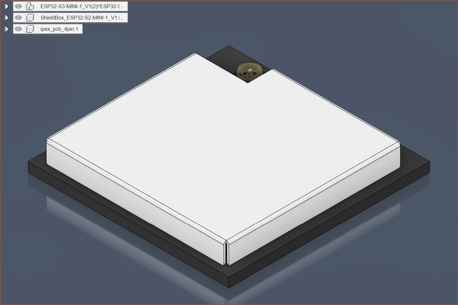
It turns out that there was a 3D model of the other version of the MINI linked in the doc PDF, so I downloaded it and edited it to bring it closer to the MINI-1U. In the PDF, it said that the connector had a diameter of 1.4mm but I could only find models of 2mm ones, so I've scaled it down to 0.7.
Footprint
Certainly the most tedious part of this entire operation.
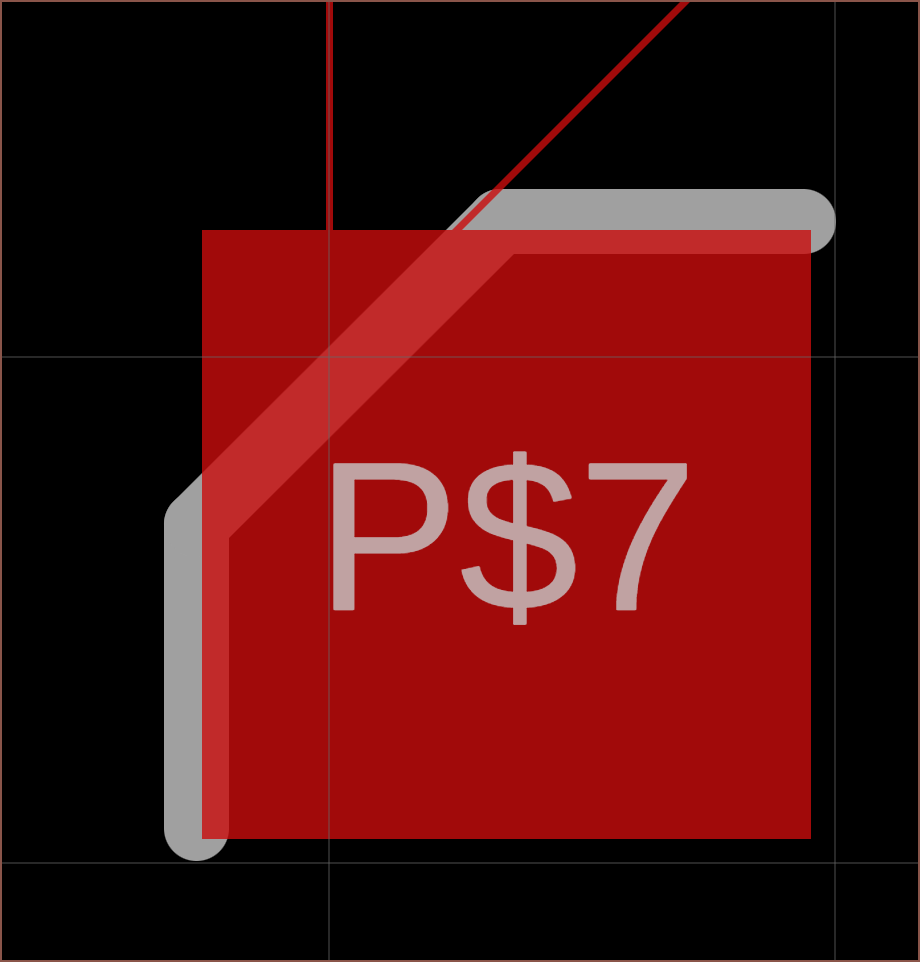
I can't figure out a way to get the chamfer for this pad. Hopefully, a fully square pad is fine.
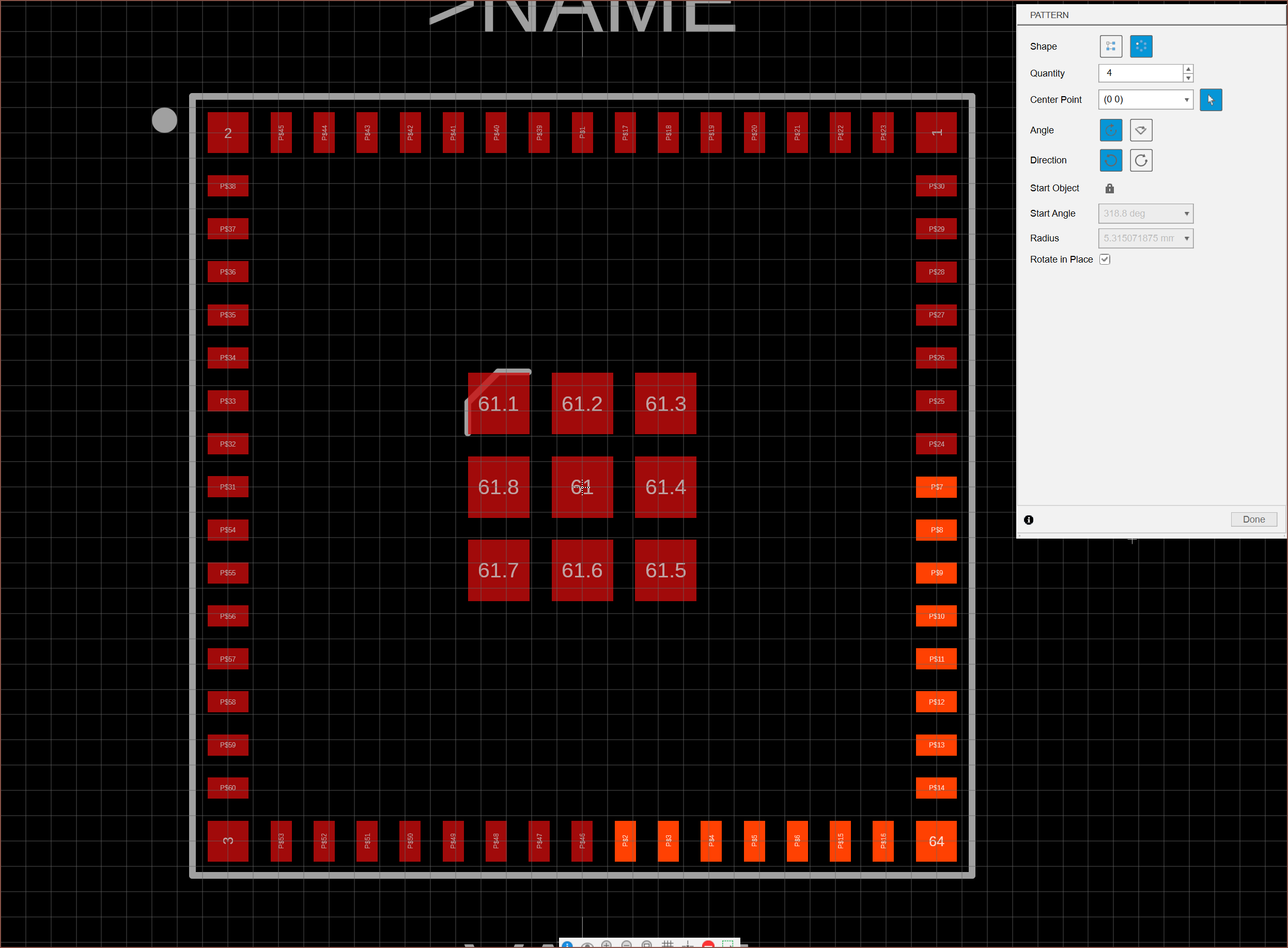
After manually calculating where the first couple of edge pins were supposed to go, I thought I could just create an upwards stack of 8 pads, rotate it around Pin 64, then rotate all of them around (0, 0). The first step worked fine, but the second step brought rounding errors:
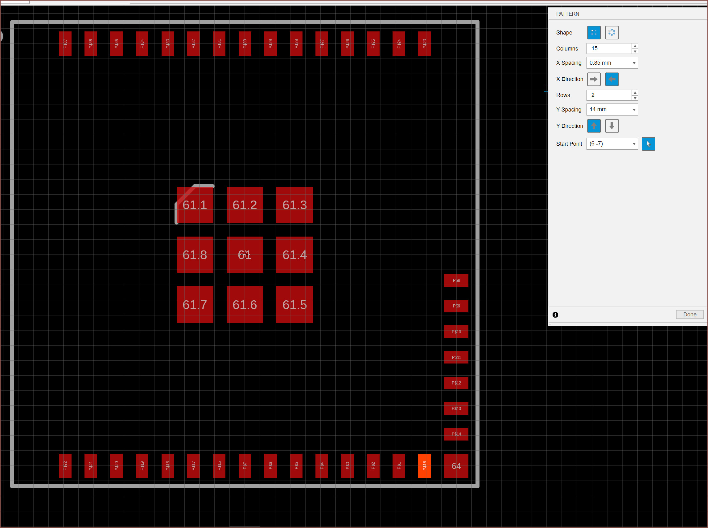
Instead, I used a linear pattern for horizontal and then vertical pins. I also used a linear pattern for the corner squares.
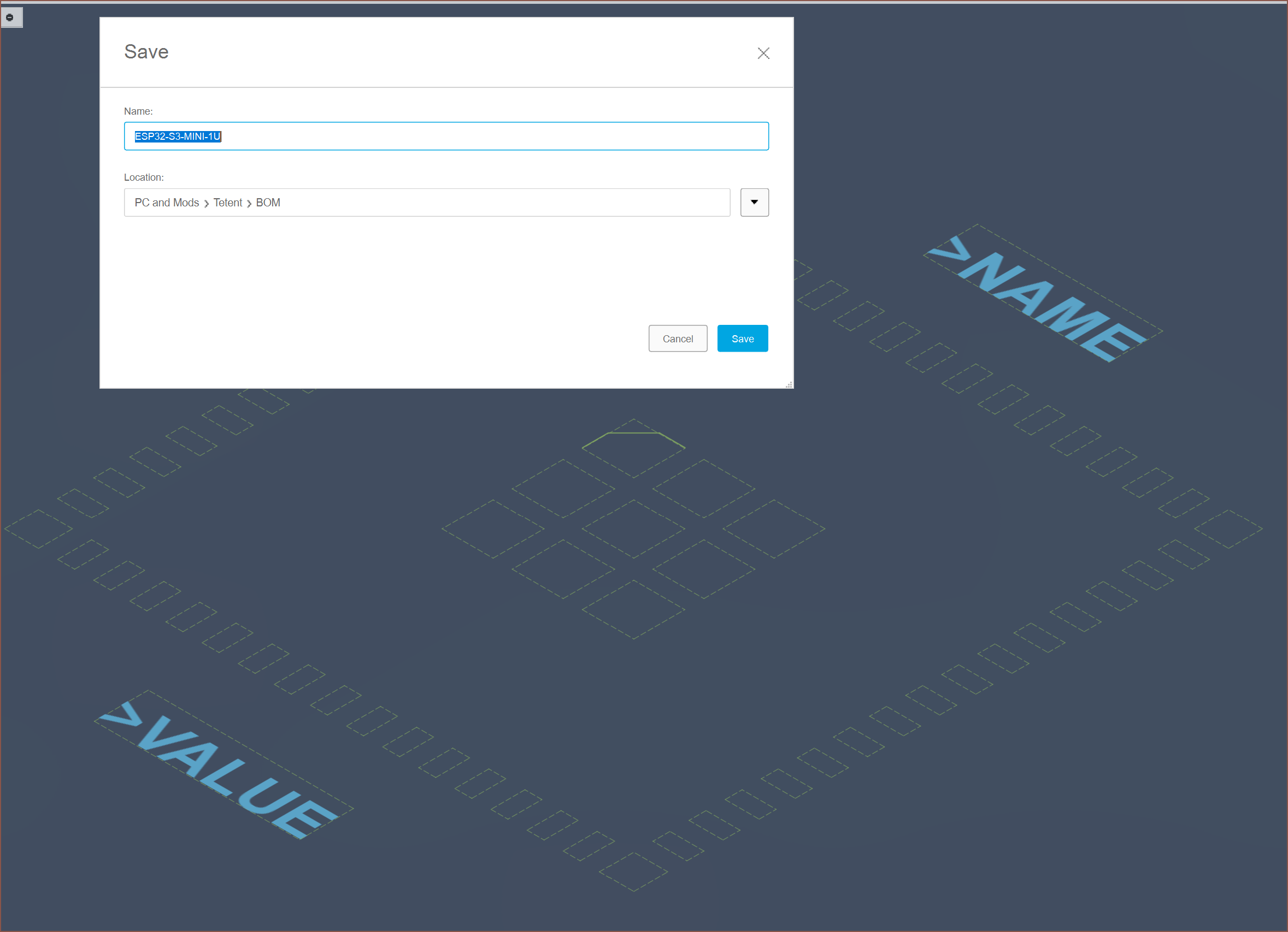
After that, I found out that I could right click the footprint and select "Create New 3D Model" to bring this up:
I still needed to save it before I could drag in the 3D model I made earlier.
It looks like everything lines up fine:
When I was linking the symbol to the footprint, I found out that I missed IO46 and added it into the symbol.
In the schematic
This is what it looks like in the schematic, so I think it's not a bad idea to have all the GPIO pins on one side. I guess this is the small benefit you get from having to make every component, though I am starting to think that this is nullifying the potential speed gains I could've had over doing all this in EasyEDA.
-
[EM] MP6543 BLDC Controller
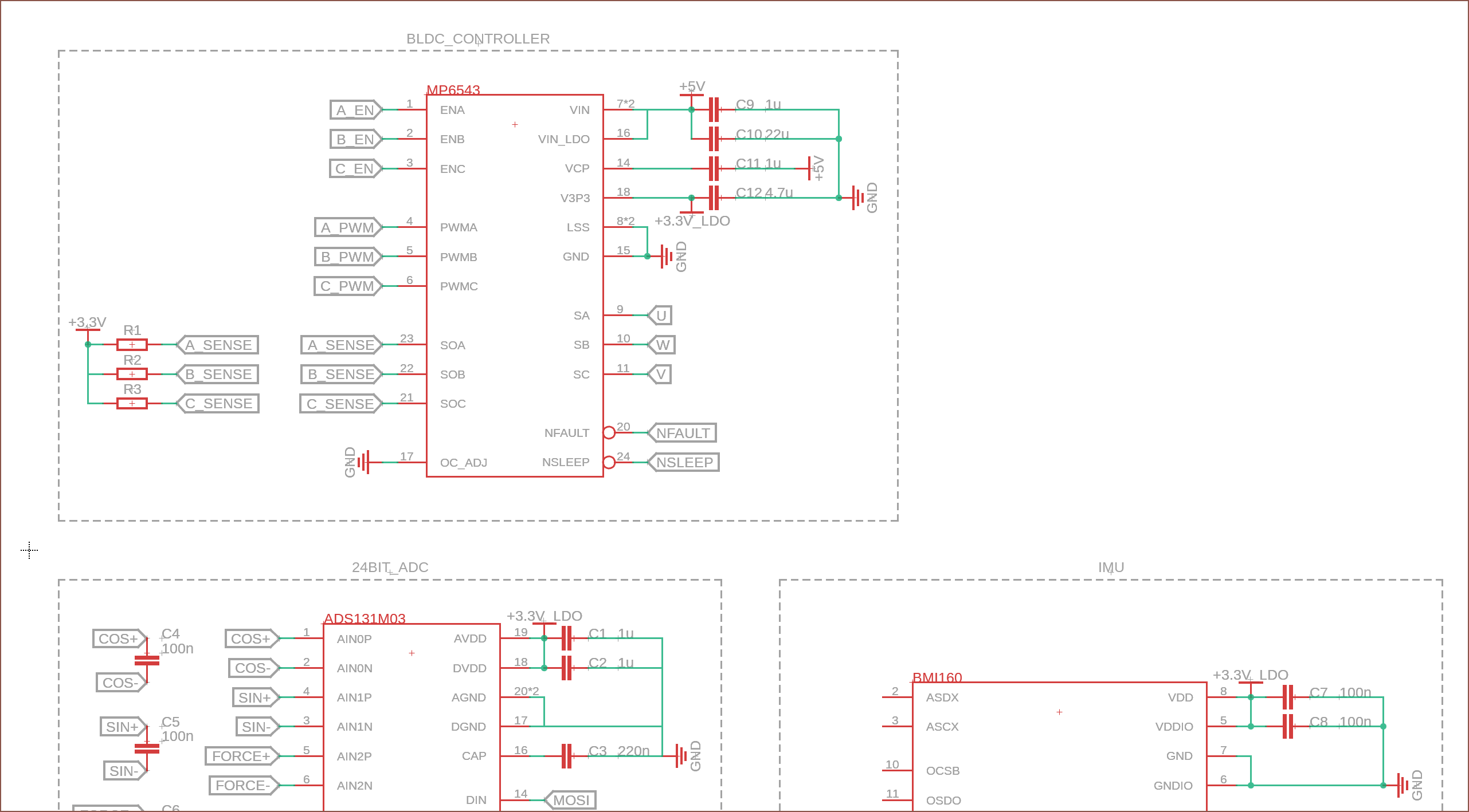
06/12/2023 at 22:06 • 0 commentsIt's about time I stopped reading about the announced-last-week Apple Vision Pro and continued creating my very own little tech innovation. I've now ported over the BLDC part of the schematic, as well as make the power sections all look consistent across all IC chips.
-
[R] Solar Cells: Polycrystaline and Amorphous
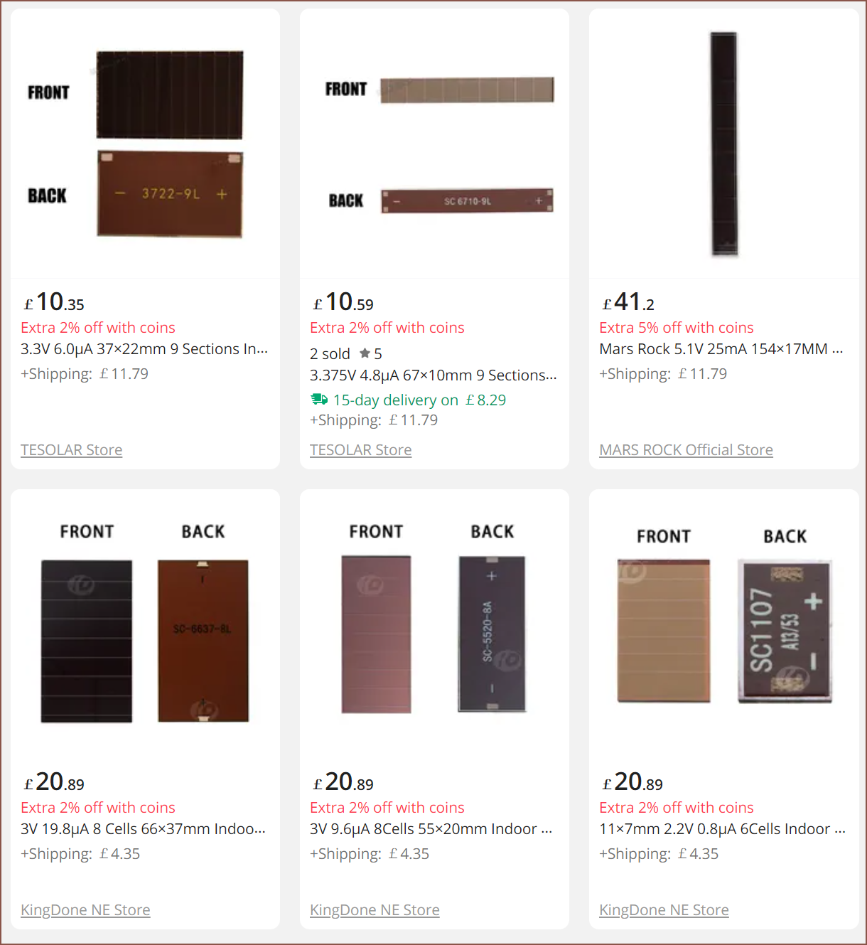
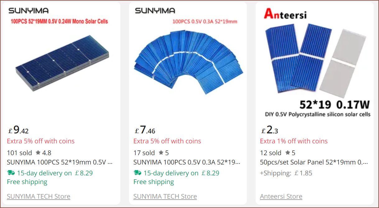
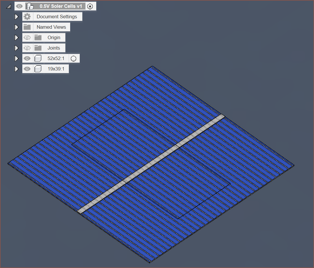
05/24/2023 at 19:00 • 0 commentsThe panel that I've just modelled in the previous log is a polycrystaline panel. I've also recently found "low light" amorphous panels, which are the reddish tint panels seen on calculators and solar keyboards. Unlike the calculators they're usually installed in, these things are really expensive on AliExpress for some reason: Take a look for these listings:
The £10 ones with £11 shipping are for 5pcs, and the £21 ones with £4 shipping are for 10pcs. Now, I looked into this and there's this video that showed the amorphus panel generating 50% more than the polycrystaline, but it was also physically larger because a polycrystaline can generate the same power as an amorphous with a smaller area if in direct sunlight.
They're also 1.1mm thick, generate voltages higher than the 0.6V from the polycrystaline and have solder pads on the back, so much easier to integrate into designs without them breaking.
The easiest source of comparison would be the 52x19mm polycrystaline vs the 55x20mm amorphous:
Amorphous 4V @ 12.3uA:      0.0492 mW
Sunyima's polycrystaline: 240.0000 mW
Perhaps this drastic difference is due to the different light intensities they were tested under?
Considering that I want to use Tetent to get more time outside and because I want all the panels to be of the same voltage level, I'll stick with polycrystaline.
-
[M] Photovoltaic cell implemented
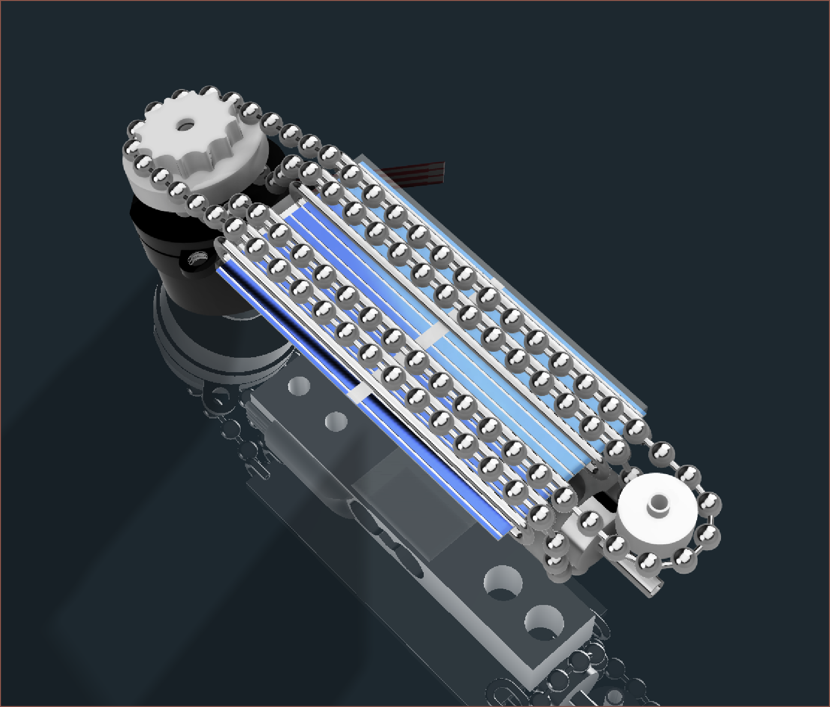
05/22/2023 at 18:50 • 0 commentsI've now been able to model in the photovoltaic cell, which is protected by a 1mm thick window.
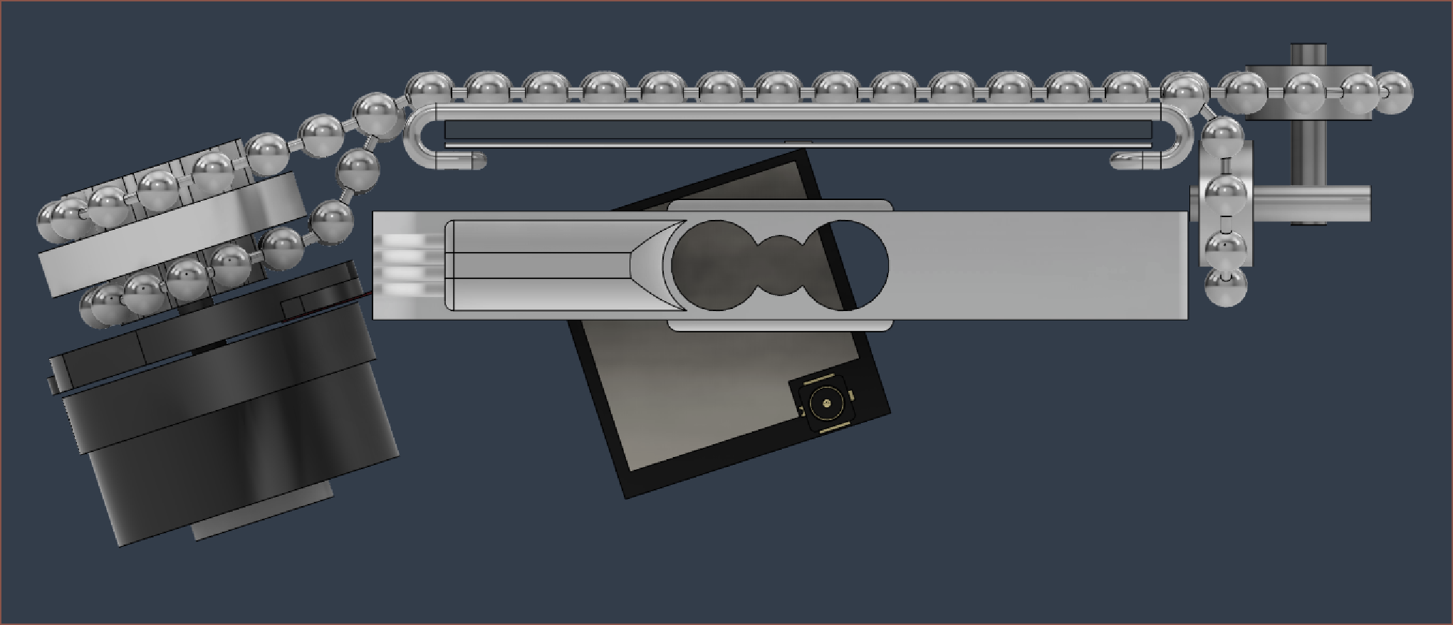
I've also brought the motor in 2mm, as well as swapped which chain goes where. As you can see in the below image, the bottom chain goes to the inside now.
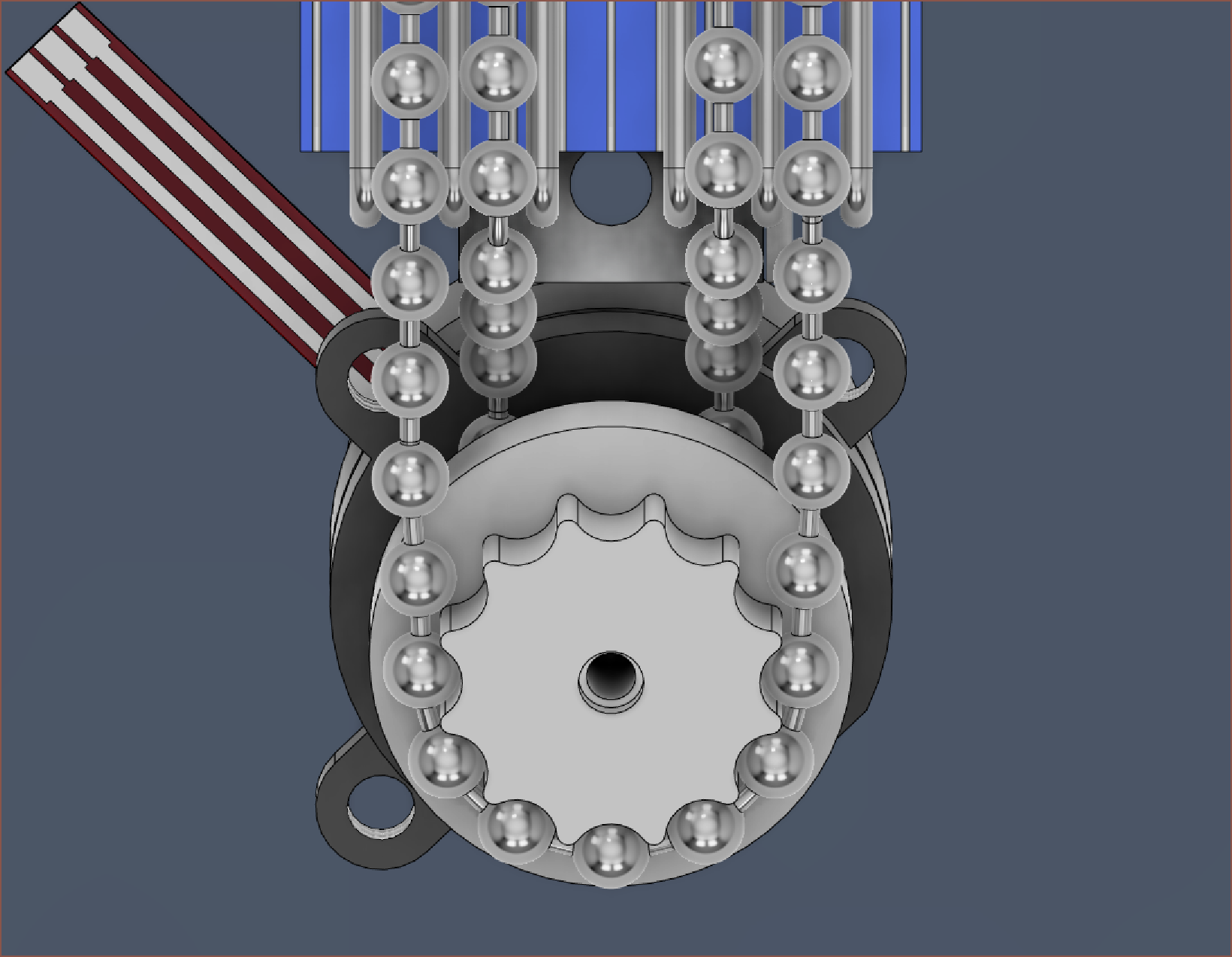
I'm still going to need to tweak the paths slightly because I'm 0.1mm off (and that's the reason why the balls look slightly misaligned). Additionally, I'm worried that it might not be physically possible to install the chain for some reason in this configuration. I've increased the amount of teeth on the pulley from 9 to 12 (in an effort to blance the paths).
The LCD looks like this with the change.
-
[M] Solar Cells
05/22/2023 at 12:42 • 0 comments -
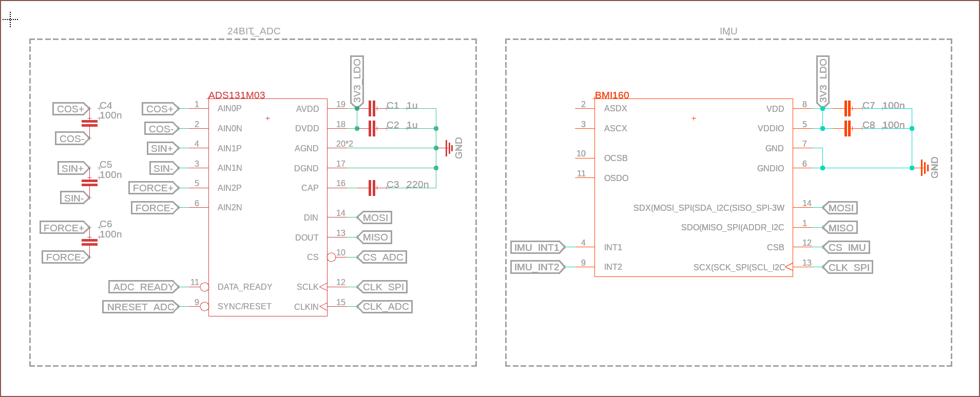
[EM] BMI160
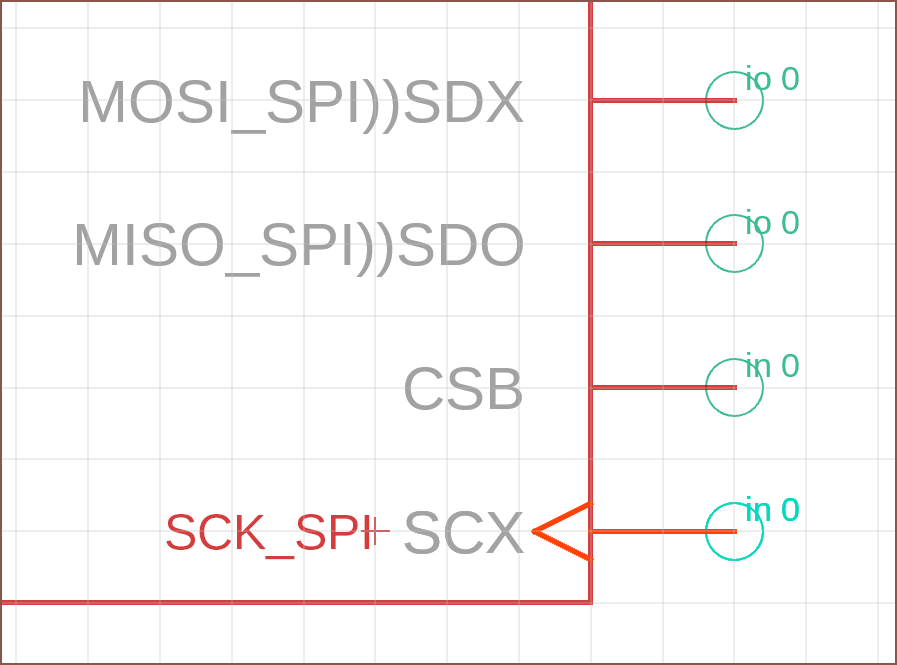
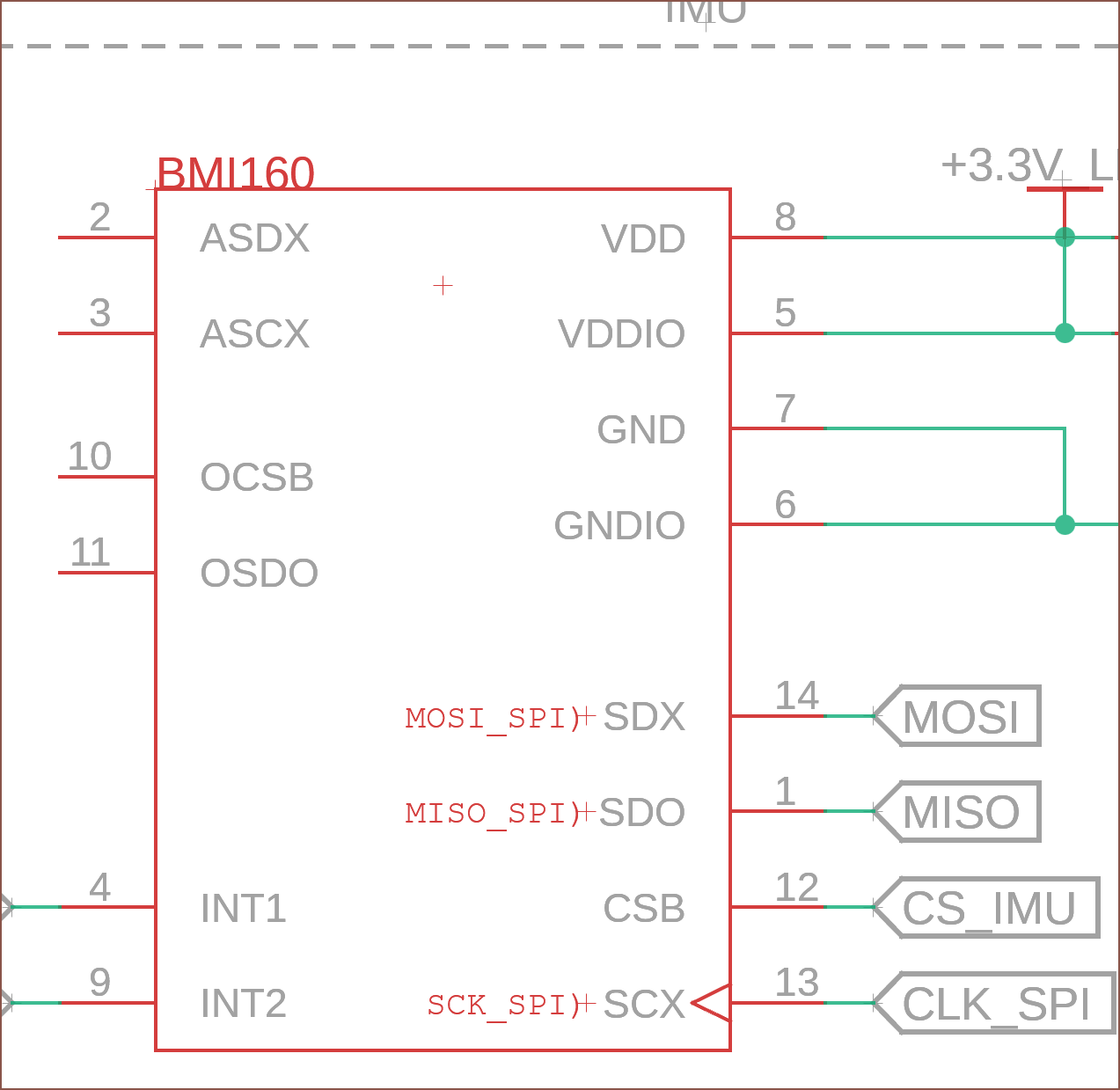
05/15/2023 at 21:35 • 0 comments- Tweaked the symbol so that the SPI part is consistent. I forgot to swap the oders of the text though.
- The interrupt pins are used for detecting different situations while using low power, so it seems important.
- I'm not sure how to set pins as NC like in EasyEDA. Perhaps it's not needed in Fusion360.
- I'm just using the circuit provided in the datasheet.
- Time taken: About 30 minutes.
Tetrinsic [gd0041]
A motorised fader that is continuous, pressure sensitive, haptic and water resistant.
 kelvinA