Close
0%
0%

Isetta TTL computer

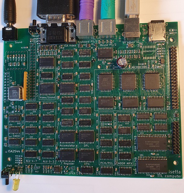
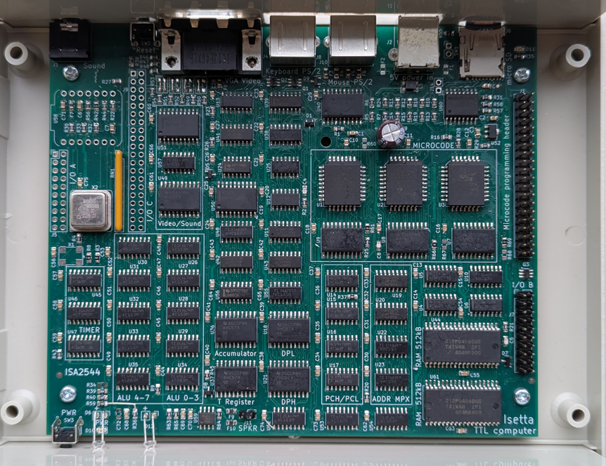
Retro computer built from TTL, with 6502 and Z80 instruction set. Includes video, sound and filesystem. No microprocessor or FPGA.

Similar projects worth following
For this project I decided to adhere to a well known instruction set. It can execute 6502 instructions and can on-the-fly switch to Z80 instructions and back.
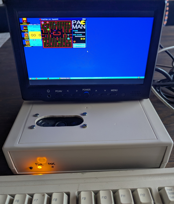
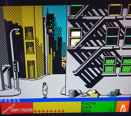
The video has 320 x 200 and 640 x 400 pixel graphics with several colors. There is no microprocessor, microcontroller or FPGA. It also has on-board file system and sound. The prototype is working and already runs ZX Spectrum games and 6502 BASIC.

The idea for this design was born at the end of januari (2023). 

While many homebuilt CPU's have their own, unique instruction set, I decided that for this project the CPU would use an existing instruction set. Also, I wanted to build the CPU from parts of the TTL family. That are integrated circuits, that can perform elementary logic functions. They were first used in the 60's of the previous age. I use a modern version of these circuits, that use less power.

So which instruction set to use ? The CPU inside your laptop or cellphone is much, much too complex to build. But it is possible to use an older CPU from the time when microprocessors just became available. There were two processors that can be regarded as the Beetle and the Deux Cheveaux of the beginning of the homecomputer age.

Those processors are the MOS Technology 6502 and the Zilog Z80

The 6502 is famous because it was the heart of the Apple 1, the Apple ] [, the Commodore 64, the Nintendo NES and many others. The Z80 is well known because it was used in the TRS-80 and the ZX Spectrum, and it was widely used to run the CP/M Operating system, see also this Z80 introduction video.

So now, I had to decide whether to use the instruction set of the 6502 or that of the Z80. But then I thought... why not build a CPU that can do both ?

I did spend a few months searching for a good design that would give good performance while not using too many parts. I think the basic design is stable now (end of march 2023). I can now start with the details of the design.

BUILD A COMPUTER

A CPU is a nice thing, but on it's own it does nothing. It needs memory, power, and input and output devices. So I planned to build a full computer. Here are the specifications:

Specifications:
 - runs 6502 programs
 - runs Z80 / 8080 programs
 - processor speed 12.5 MHz (80nS cycle time)
 - 512 kByte RAM ( 8 bit wide )
 - 24 bits wide microcode in 3 flash chips 
 - programmable (upgradable) microcode
 - on-board SSD file system 32 Mbyte
 - video VGA 320 x 200 pixels, 64 colors for each pixel
 - video VGA 640 x 400 pixels, 16 colors for each pixel
 - PS/2 keyboard connection
 - PS/2 mouse connection
 - Serial connection for file transfer (to Raspberri Pi)
 - Connection for ESP-WROOM-02D WiFi card
 - Connection for micro SD card
 - real-time clock synchronized by WiFi
 - sound generator
 - blinkenlights (4)
 - general purpose I/O
 - pcb 119 x 150 mm  (4.7 x 5.9 inch), 4 layers.
 - powered by 5 volt USB input (250 mA)

 Components:
 - RAM memory chip
 - Three Flash memory chips
 - SPI Flash memory chip for mass storage
 - 51 TTL logic chips (38 CPU, 9 Video and I/O, 4 Bankswitching)

 Principles for the design:

 - No microprocessor, microcontroller, SOC, FPGA, CPLD, GAL, PAL or 74181
 - All components have good availability at the big distributors
 - Low number of components
 - No fine-pitch devices that are difficult to solder

WHAT CAN IT DO ?

At the moment (aug 2024) it can:

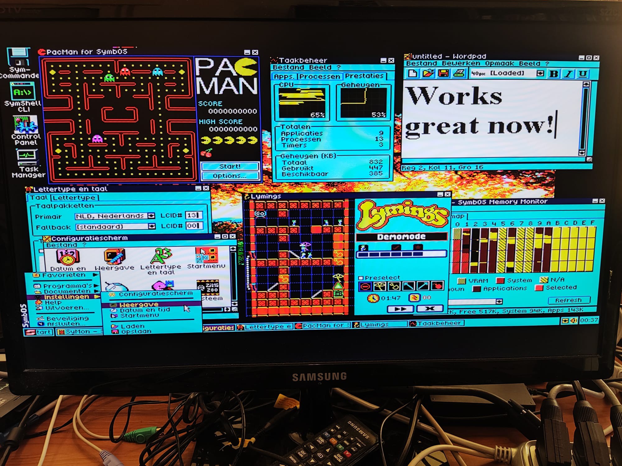
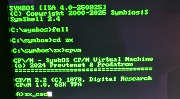
Several more applications are planned. Having a nice operating system is one of them.

SELLING KITS

Soon there will be a KIT, to build your own Isetta !

DISCUSSION

For questions or tips/remarks you can use the discussion section at the end of the main page.  Or you can join the discussion at the RetrocomputingForum / Isetta. BTW, where do you come from ?

Flag Counter

ISETTA SYSTEM DIAGRAM

CLAIM

There are many homebuilt CPU's on the internet. But I never saw a homebuilt CPU with a Z80 instruction set (FPGA designs or emulations don't count). Therefore,

I claim that this is the very first homebuilt CPU that can execute Z80 instructions (August 2024). ...

Read more »

isettos 250116.bin

octet-stream - 127.56 kB - 01/16/2025 at 20:28

Download

microcode bin 250112.txt

plain - 896.01 kB - 01/12/2025 at 10:04

Download

symbosvm 250111.bin

octet-stream - 127.56 kB - 01/11/2025 at 12:48

Download

microcode bin 250103B.txt

plain - 896.01 kB - 01/03/2025 at 15:20

Download

microcode bin 250103A.txt

plain - 896.01 kB - 01/03/2025 at 15:06

Download

View all 35 files

  • Announcing kits on the last day of 2024 !

    roelh12/31/2024 at 12:44 0 comments

    Both prototypes that I have built worked without any HW problem (of course there were SW problems now and then). On the first one, I ran The Great Escape (in its self-running mode) continuous for almost a week. This gives confidence.

    SELLING KITS

    I could now soon start with selling kits.  If you are interested, let me know in the comments or in a private message.

    The price of the kit will be around 100 Euro (USD 110) (Shipping costs not included). You will need to have some experience in building electronic kits.
    - You buy the bare pcb from me, for 30 Euro. I will make instructions and a detailed list of parts.
    - You buy all parts from an electronic parts supplier, like Mouser or Digikey. Cost around 65 Euro, free shipping at several suppliers.
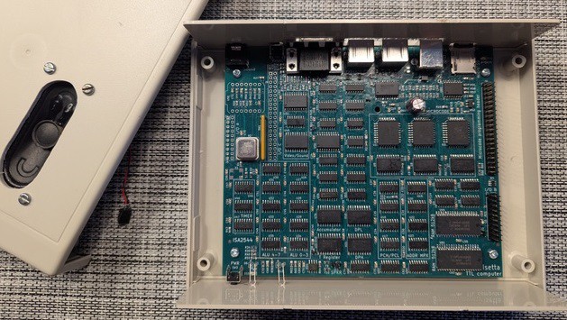
    - An enclosure is not yet included. But the pcb is designed to fit in a Hammond RM2055S enclosure.

    Selling complete Isetta's might come later.

    What more do you need

    You need several other things, that you might have lying around:
    1. A universal programmer to program the three flash chips with microcode. Or the Isetta programmer pcb.
    2. A Raspberry Pi (RPi), for transferring files to the 32MB on-board storage of Isetta
    3. A 5 volt power supply with USB-B plug
    4. A monitor (CRT or LCD) with VGA connection, with cable and 15-pin connector
    5. A PS/2 keyboard
    6. A PS/2 mouse (not needed for all applications)
    7. A micro-SD memory card (might be needed by some applications)
    8. A speaker with amplifier, with 3.5mm (stereo) plug. For sound.

    Programming the microcode

    You can use a regular, universal programmer to program the microcode in the three flash chips (PLCC44 case). (I have not done that myself yet, I use the RPi). But, it is very likely that new microcode versions will appear, so you have to use sockets on the pcb to be able to reprogram them. Sockets can be unreliable, however.

    You can also use the special Isetta programmer pcb (that I will sell you for 10 Euro). It needs 11 TTL chips, and connects the Isetta to the Raspberry Pi. The Raspberry Pi can now program the microcode flash chips while they are soldered on the board. The programmer pcb also allows the RPi to send files to the on-board storage, and allows low-level testing and single-stepping the Isetta. The low-level testing is VERY useful if you soldered your own Isetta.

    The RPi also needs a monitor (HDMI connection), USB keyboard, and power supply.

    Note that, as soon as the microcode is programmed and files are transferred, Isetta can work fully stand-alone without needing the RPi or the programmer pcb. In the future, Isetta should be able to fetch files from the micro-SD card, or through its WiFi connection.

    If you only need file transfer, you can connect the RPi with 4 wires to Isetta, without needing the programmer pcb.

    Future plans

    - Make a good description of the available I/O instructions
    - Provide more microcode support for writing to the screen
    - Implement a nice sound generator
    - Support micro-SD card and WiFi
    - Have an editor/assembler on Isetta
    - Add applications
    - Have a nice operating system

    I could use help ! But you'll first need the hardware...

    What did I do since the last log ?

    - Write text to the new 640x400 screen
    - Implement the RST #38 interrupt (interrupt mode 1) at each video frame. Can be enabled/disabled with EI, DI instructions.
    - Made a mouse driver in microcode. An I/O instruction can now read messages from the mouse.
    - Completed several changes that were needed due to HW changes on the new pcb
    - Created an output instruction to do bankswitching

    END OF THE YEAR

    Best wishes for the new year ! That you and your loved ones all be happy and healthy !

  • New pcb, new video mode

    roelh11/17/2024 at 13:07 0 comments

    A few weeks ago I received the new pcb (ISA2442). Several things have changed with respect to the first pcb, so several software things had to change.

    One of the main changes was the 640 x 400 pixel mode. On the first pcb, a byte from memory represents 8 pixels, and the byte tells for each pixel if it has foreground color or background color (these colors being programmable).

    On this new pcb, a fetched byte has information for only two pixels (pixels last 40nS). So we can simply have 4 bits (16 colors) per pixel. The color of each of the 256000 pixels can be set independent from the others.

    Today I got this new mode to work. 
    On the picture you see mainly uninitialized memory, that gives a random, noisy pattern of colored pixels.
    In the first row I programmed the 8 basic colors, and the second row shows the same colors with low intensity. So the upper two rows show all 16 available colors in this mode.

    On the last row I made horizontal and vertical stripes, and a few checkerboard-patterns of two colors, that give the 
    impression of another color (orange, and variants of green and blue).

    You might ask why this is only 400 lines instead of the standard 480. This is because the processor can not run the user program during the active part of the video frame, because it is busy rendering the screen. By using only 400 lines, the processor has more time to run the user program.

    The 320 x 200 pixel mode (used for the ZX Spectrum screen) was essentially unchanged. 

  • Second PCB version ordered

    roelh10/19/2024 at 08:49 1 comment

    Yesterday I finally ordered the new PCB. This PCB is sponsored by the kind people of PCBWay, the well-known high-quality PCB fabrication company from China. During production you can always check in which production state your pcb is, and I watched an impressive series of videos that show all steps in the production process.

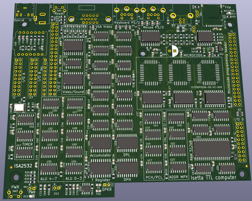
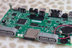
    This is the KiCad 3D-impression of the new PCB:

    With respect to the first PCB, the main changes are:

     - fix mistakes (VGA connector)
     - add Mouse connector
     - add HW for sending info to keyboard (and mouse)
     - add memory bank select
     - change video pixel/color generation for 640x400 mode
     - change WiFi module type
     - simple 4-wire connect to Raspberry Pi (for file transfer)
     - instead of a SPI header, a micro-SD card connector is mounted
     - changed SPI reading, it can now be done in 2 cycles/bit (instead of 5)

  • Changed bankswitching system

    roelh10/14/2024 at 12:59 0 comments

    In this previous log I described the new bankswitching system. But I wanted to add another mode (Linear mode). It would be nice if a program could access the whole 512kB memory without bankswitching. The address would be in a 3-byte register, with 19 significant address bits. A simple processor with 19-bit addresses could then be implemented.

    For programming the Z80 or 6502, it is not needed to know all this. You only need this if you implement a bankswitching system or a new processor microcode that accesses the whole memory. Probably it is only for myself.

    I came up with the following: (All images can be enlarged by clicking them)

    LINEAR MODE

    The functions are essentially the same as in the mentioned previous log, but I added the Linear mode. For program code, the upper bits A18 and A17 come from a bank select register, and A16 comes from microcode. For data, upper bits A18, A17 and A16 come from another bank select register. So, the upper three address bits can be different for program and data. Also new is, that this bank select register can be loaded from a memory-resident register in a single cycle.

    APPLICATION and KERNEL

    It is intended that, for Application and Kernel modes, BS_2 and PC18 are always written with the same value. That makes our table slightly less complex:

    This diagram shows all modes. The modes are controlled by signals in the microcode and the bank select registers, as shown.

    HARDWARE IMPLEMENTATION

    The result is a bit complex because I didn't want to add more chips. Another complication is, that the address must be available quite fast, so there can not be long propagation delays. The following diagrams (there are seven) explain all modes, and also the way it is implemented. The used colors are the same as in the table above.

    You find the bankswitching control registers at the top of the diagram. The microcode control signals are at the left side. At the right side, you find the five highest address bits, their value indicated by '0' or a color.

    REGISTER MODE

    This is the simplest. The (memory resident) registers are in the very first 256 bytes of memory. This mode is selected by CTL_M1 = 1. The CTL_M1 signal switches all upper address outputs OFF, so all upper address bits are zero. The register in question is selected by several bits in the microcode.

    The value in the bank select registers is irrelevant.

    TABLE / ZPAGE

    In this mode only the lower 8 bits of a data or code address are used. The other bits are zero, but A16 and A17 come from microcode. It is used for 6502 Z-page, for an identity table and a shift-right table. If A16=0 and A17=0, this mode can not be used (that is the domain of the memory-resident registers).

    This mode is selected by microcode signals only. The value in the bank select registers is irrelevant.

    NATIVE

    This is the main addressing mode of the first prototype. The upper address bits are 'hardwired' in the microcode. Bit A18 can no longer be used, that should not be a big problem because this will no longer be the main addressing mode.

    This mode is selected by microcode signals only. The value in the bank select registers is irrelevant.

    APPLICATION MODE

    Here, the upper three address bits are freely programmable in the bank select register U50. It is advisable to set BS_2 equal to PC18, otherwise the topmost address bit is different for code and data (also for the following two modes kernel slot1/slot3).

    This mode is selected by microcode signals in combination with APPL = 1. Yes, the APPL signal got it's name from this mode.

    KERNEL SLOT1

    The 64k addressing range is split up in four slots:

    • Slot 0 ( 0000 - 3FFF )
    • Slot 1  (4000 - 7FFF)
    • Slot 2 (8000 - BFFF)
    • Slot 3 (C000 - FFFF)

    In this kernel-slot1 mode, normally the microcode selects which 64k bank is selected (orange signals). But if the address is in slot 1, the bank number comes from the bank select register (light...

    Read more »

  • Fixing the LDIR instruction

    roelh09/17/2024 at 20:18 0 comments

    In the past weeks, I've been working on a new pcb design. That's now almost done.

    This weekend I looked at my TODO list, and I found, no surprise, the LDIR instruction.

    In one of the previous logs I mentioned that there was an error in the LDIR instruction. It didn't behave correctly when an interrupt occurred.

    What is the LDIR instruction ? 

    In the Z80 processor, this instruction can copy a whole section of memory in just a single instruction. It takes three 16-bit sized values as input:
     - A source address in register pair HL
     - A destination address in register pair DE
     - A byte count in register pair BC

    LDIR stands for Load, Increment, Repeat.


    It will do the following actions:
     - read a byte from the address at location HL
     - write that byte at location DE
     - increment the addresses in HL and DE
     - decrement the byte counter in BC
     - if the byte counter is not zero, repeat the actions
     - if an interrupt occurs during this instruction, it will be handled and the actions will continue after interrupt is handled.

    LDIR has a 2-byte opcode: ED B0

    Optimizing the LDIR

    The LDIR was already optimized, with 10 cycles per copied byte, but I had the strong feeling that something better was possible. I didn't try to find the problem in the old version, just started again from scratch.

    Isetta has only a single hardware data pointer. But nothing keeps us from using the program counter as a data pointer ! For a normal instruction, that would cost way too many cycles, but for a repeated transfer instruction this will pay off. The LDIR microcode should just save the PC to a temporary location, and copy the HL register pair into the PC. Now the PC can be used to get the bytes out of memory. When all actions are completed, the PC is copied back to HL, and PC is restored from the temporary location. The existing, broken LDIR version also had this feature.
    And as a bonus, the PC register can increment in the same cycle where it addresses a byte to be fetched.

    The destination pointer (register pair D E) is copied to the hardware registers DPH and DPL. The byte, fetched with the address in PC, can now be stored at the address in DPH/DPL. There is a microinstruction that increments DPL, it can also detect a carry, but there is no possibility to increment the DPH register, because it can not be accessed after the change that is described HERE. But we could increment the D register and re-write DPH with the result. This will at least take 3 more cycles (microinstructions).

    Then we must decrement the count in the BC registers. So first decrement C (2 cycles) and, when it drops below zero, decrement B (also 2 cycles). 

    The problems are in the counting, and in the increment of the upper byte (DPH), 

    But if we unroll the loop, in sections of 8 transfers, we don't have to count each byte. We simply subtract 8 from the LSB of the count, at the beginning of the unrolled loop. But when the count is lower than 8, we jump to a slow old-fashioned loop. This will decrement the MSB of the count when that is needed, and then go back to the unrolled loop. The slow loop will also check for zero to determine if the instruction has completed.

    It would be nice if we never had to increment the upper byte (DPH)...  What if we never increment the upper byte in the unrolled loop ? Before the unrolled loop starts, we could check if the lower byte (DPL) would overflow in that loop. That would happen if that lower byte is higher than 0xF7 (247), and in that case we do the old-fashioned loop, and when the upper byte has been incremented, we go to the unrolled loop again.

    Now, the sections of the unrolled loop have only 3 cycles:
     - A <- (PC++)
     - (DPH/DPL) <- A
     - inc DPL

    Pseudo code of the fast copy loop:
     - if LSB of the count < 8, goto slow loop
     - if LSB of destination > 247, goto slow loop
     - count = count - 8
     - copy the DE registers (destination)...

    Read more »

  • Progress of new PCB

    roelh09/07/2024 at 10:14 0 comments

    Here is an impression of the new PCB (Image generated by KiCad). It's almost finished.

    And here is a small section (of four IC's) :

    The TOP layer is RED, first inner layer is groundplane (not shown), second inner layer is ORANGE and the BOTTOM layer is BLUE. You can click on the picture for a better view.

    Yes, all routed by hand.

  • On the cover of the hack a day

    roelh08/31/2024 at 18:12 5 comments

    The Isetta made it to the front page !

    The Computer We All Wish We’d Had In The 8-Bit Era by Jenny List.

    We take all kind of pills
    That give us all kind of thrills
    But only one thrill is gonna stay 
    Thats the thrill that you'll get when you find your project
    On the cover of the hack a day


    (Hack a Day) Wanna see my project on the cover
    (Day) Made a big printout just for my mother (yeah)
    (Day) Wanna see my smilin' face
    When my project is on Hack a Day

    Thank you, Jenny !

    Understand a little Dutch ? We've got you covered. There is a nice cover of the cover....

  • Hardware changes and bankswitching

    roelh07/28/2024 at 15:30 0 comments

    Luckily, the first prototype worked without real problems. The only obvious one being the strange footprint for the VGA connector. 

    But for my next pcb run, I want to do several changes:

     - fix mistakes (VGA connector)
     - add Mouse connector
     - add HW for sending info to keyboard (and mouse)
     - add memory bank select
     - change video pixel/color generation
     - change WiFi module type
     - simple 4-wire connect to Raspberry Pi (file transfer)

    BANKSWITCHING

    The memory bank selection is, I think, the most complicated of this new features. The new system will have the following modes: Register, Table/ZPage, Native, Application, Kernel slot1, and Kernel slot3. You can see that in the following table:

    In the current hardware, only the Register mode, Table/ZPage and Native mode are present. The register mode allows access to 64 fixed locations in memory (a kind of zero-page addressing). There is another group of 64 locations that can be switched (for Z80 registerbank switching). Table/ZPage mode is used with an identity (1:1) table to access DPL and PCL, to access the Shift-right table, and for the 6502 to address ZPage values. The Native mode allows addressing the full 512 Kbyte of memory, but it's problem is, that the used 64K bank (yellow fields) is hard programmed in the microcode.

    This will now be more flexible. In the new Application mode, one of the 8 selectable 64K banks can be programmed in a bank select register (blue fields). The selected bank will be valid for data as well as program code. Note that the microcode can force that Native mode or Register mode is used, by using the control bits CTL_M1 or CTL_REG2.

    An operating system must be able to access all memory, to be able to load programs and move data around. I want to adhere to a common practice in several Z80 systems, where the memory space is divided in slots of 16Kbyte. To make this not too complicated, only 2 of these 16Kbyte slots can be mapped to another 64k memory bank.

    So, the Kernel_slot1 mode allows you to map any of the 32 blocks of 16kByte into slot 1 . Eight banks of 64K can be chosen with the blue BS signals, while within such a 64K bank, a 16K block can be chosen with the orange BLK signals. Slot0, 2 and 3 will select the 64K bank that is defined in the microcode instruction (with the yellow BNK signals).

    The Kernel_slot3 mode allows you to map another block in slot3. But this has a few restrictions. The mapped-in block can be any 64K bank, but within that bank it is always block3. And no code can be executed from the mapped-in block.

    In the table, the bits indicated in RED show which bits are needed to select a certain mode. For the bank select register, there are only 3 types: Application/Native, Kernel_slot1 and Kernel_slot3.

    VIDEO CHANGE

    In the current video system, in the 640-pixel mode, a byte from memory represents 8 pixels, and the byte tells for each pixel if it has foreground color or background color.

    But this system was designed when the processor/memory cycle was still 160nS.

    Now that I changed the cycle time to 80 nS some time ago, a fetched byte only needs to provide color for two pixels (pixels last 40nS). So we can simply have 4 bits (16 colors) per pixel ! Now each pixel can have an independent color.  This seems much more flexible than the previous system, so I'm gonna change that. 

    VGA connector footprint issue

    It turnes out that all KiCad footprints for these DSUB-15HD connectors are wrong, and that was known already 5 years ago, see this issue report. Swiching to the newest 8.0 version still had the wrong footprint. So I had to edit the footprint myself.

  • Two Spectrum games working

    roelh06/27/2024 at 20:39 0 comments

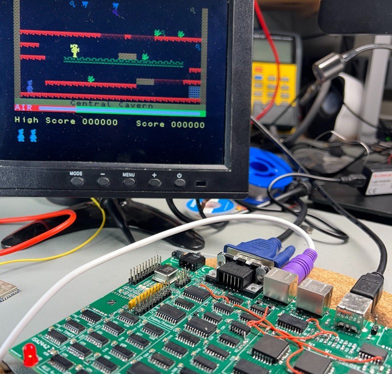
    After a little while, I got the Manic Miner fully working, including sound:

    But in the video signal, there are two annoying stripes at the right side of the screen (also going through the score). This is related to a end-of-line flag that is tested there in the microcode that builds the screen. The exact reason is not known yet. [ edit: the reason was found, and the bug removed.]

    SOUND

    The sound took a little fiddling to get it to work properly. The ZX Spectrum has a very simple sound system, similar to that of the Apple II. It is a single bit of an output port (port 0xFE), that is amplified with a single transistor, and connected to a small speaker. The program has loops that toggle that bit with a certain timing.

    The Z80 of the Spectrum runs at 3.5 MHz. Isetta runs at 12.5 MHz. But Isetta spends around 73% of her time rendering the Spectrum screen, so her effective speed is about 3.375 MHz. A Spectrum program, generating a constant tone, would come out as a series of high-frequency 'chirps' during blanking time.

    The write to the 0xFE output port is handled by microcode. It now stores the value instead of writing it to the speaker. At every line interrupt, this value is put in a buffer (only during blanking time when the Z80 code runs, that is about 140 lines per frame ). But in every line interrupt (525 times per frame), a value is read from the buffer and written to the sound output. The same value is used four times, and then the buffer pointer is incremented. So the sound is stretched by a factor 4.

    It had another problem. The sound bit is normally zero, then it toggles during the tone, and then is zero again. This means that it has a low-frequency component. In the ZX with its tiny speaker this was probably no problem, but in my case I have a set of amplified PC-speakers (with 3.5 mm jack connector) that have a 'good' bass response. So the little 'music' tones were accompanied by loud plop sounds.

    The sound system of Isetta has 8-bit samples. I defined a level that was halfway the 0 and 1 of the speaker signal. So normally the signal was at 50%. When port 0xFE was written, the signal would be 0% or 100 %. But the point is, it is difficult to know when the tone stops, so you don't know when to go back to 50% . I did this as follows. At each interrupt, when the 0xEF port was not written, I bring the speaker signal a few steps closer to 50%. So when the tone stops, the signal will go to 50% quite soon. This gave a reasonable sound quality.

    KEYBOARD

    I already had Z80 code to convert the PS/2 keyboard to ASCII, and to convert ASCII to the codes for the ZX Spectrum keyboard matrix. But for playing a game, I also had to use the PS/2 'key released' messages, to tell the game program exactly when a key was released. 

    THE GREAT ESCAPE

    I tried another program. The Great Escape. This program also has a very good, commented disassembly

    In this program, a prisoner of war has to escape from a prisoners camp. It is totally different from the previous game.

    The display is a semi-3D rendering. It is almost a modern game, where a camera follows the hero on the terrain and in the several buildings.

    It did not take much time before I saw the first guards walking on the screen. But it was only a few second, then the program crashed. What could it be ? I looked through the source and I found it used an instruction that I had not implemented, because my thought had been, who is ever going to use that ??  RRD  Rotate Right Digit

    But the game uses it to shift the whole screen four pixels to the left or the right....

    So the RRD and RLD are now also in the microcode.

    Program worked. But I have no clue how to escape...

    [ edit: What David Thomas says about the great escape ]

  • Trying to get a ZX Spectrum game running

    roelh06/14/2024 at 14:44 0 comments

    TEXT MODE

    In the last log I mentioned that there was video output.

    A 80-column text mode was created. Each character is in a 8 x 8 pixel matrix. To make it better readable, a few empty scanlines are between the textlines. The VGA pixels are generated by the microcode.

    At the moment this is mainly used as a text mode, although it is actually a graphic mode with 8 bytes of 8 pixels each. For each row of a 'character', there is also a color byte. The idea is that every character can have a different color (but since this is a graphic mode, each row of a character could have it's own color). The background color for a character can also change, but that's not fully implemented yet.

    The picture shows how the system starts in the current version. It shows a few big colored fields to show some of the colors. At the right side you see some random colors, where you can see that each character can have a different color for each row.

    You also see how the file directory shows up. A line that starts with "D" means that this is a directory.

    After I got this video mode working, I worked on the PS/2 keyboard input. The keyboard did only give a singe message after startup, always the same, and did not respond to key presses. After searching my keyboard on the internet, I found that some keyboards need a RESET message before they start working. In my case, I had to solder two transistors on the pcb to be able to transmit the reset message to the keyboard. But then it worked ! A Z80 program translates the scancodes to ASCII. 

    Isetta can now run with its own keyboard, video output and file system, without the need for the RPi !

    ZX Spectrum video system

    After I got that working, I spend some time making a video mode that behaves as ZX Spectrum graphics .

    To test this, I downloaded the source of the game Manic Miner. I could only get this to work if I also found the explanation of Manic Miner source code. Here is the first result:

    Obviously, not everything was working correctly yet. There were vertical lines at every character boundary, and apparently the attribute bytes of the lower part of the screen were not correct.

    It could be traced (within reasonable time) to a failing LDIR (load-increment-repeat) instruction. This is used in the game to copy big blocks of bytes to the screen, with a single instruction. The LDIR, that is implemented in microcode, was designed to check for an interrupt periodically, and in the case of interrupt set the program counter two steps back, and after the interrupt resume the copy operation. But it didn't work correctly with interrupts.

    The LDIR was a highly optimized piece of microcode. At ten cycles per transferred byte, it loaded the byte, stored it at the destination, incremented the HL source address (with carry between low and high byte), do the same for the DE destination address, decrement the BC byte counter, test if BC is zero. And also check the interrupt signal at every transferred byte.

    I took the fast way out. I grabbed a RST instruction (0x20) and did put a copy routine there. In the source of the Manic Miner, I replaced every LDIR with a RST 0x20. Followed by a NOP to leave addresses unchanged. Getting the bug out of the LDIR instruction was put on the TODO list. Now I got this:

    Already much better !

    I could also see on the piano keys that the start-up tune was playing (but of course I have no sound yet). Also, a scrolling message was visible. After that, the program crashed. More debugging to do !

View all 31 project logs

Enjoy this project?

Share

Discussions

Paul Driver wrote 08/31/2024 at 21:41 point

Dr Matt Regan on YouTube has an entire series on microcoded TTL computers, and has done 6205 emulation, culminating in an Apple II clone) as well as the Z80, culminating in both Sinclair ZX80+ and Spectrum clones.

https://youtube.com/@drmattregan?si=3HBWGR9niP8KzCvZ

  Are you sure? yes | no

Eric Hertz wrote 09/01/2024 at 02:03 point

Dr. Phil might have something to say about someone who has to spam every corner of another's creation...

The one in the "On The Cover of Hack A Day" log-entry really takes the cake.

  Are you sure? yes | no

roelh wrote 09/01/2024 at 07:26 point

Hi Paul, in his video https://www.youtube.com/watch?v=y04AH5Q3Z3I  Dr Matt Regan shows his Z80 TTL system working. But he only implemented a (small?) part of the instruction set. It's not clear which instructions he implemented and which he left out. But his demo can only show the copyright message at the start of a ZX81. This could be done with less than 10 different opcodes. Isetta can handle more than 650 different opcodes for its Z80 mode.

His Sinclair Spectrum clone uses a regular Z80 cpu (https://www.youtube.com/watch?v=N36iWYcXBAE) and not a Z80 built from TTL.

  Are you sure? yes | no

Con Cunningham wrote 04/21/2023 at 21:11 point

Just  been reading your square inch TTL CPU - great work. Did you publish your microcode, or is that proprietary ? Curious how you managed such a rich ISA with so few control signals!

  Are you sure? yes | no

roelh wrote 04/22/2023 at 18:08 point

Hi Con, the microcode can be seen when you scroll down on the simulator page: 

http://www.enscope.nl/simas_nac/

Did you read the logs ? If you also look at the schematic,  ( https://hackaday.io/project/161251-1-square-inch-ttl-cpu/log/154913-schematic-of-the-cpu ) you should be able to understand how it works.

  Are you sure? yes | no

Con Cunningham wrote 04/21/2023 at 20:51 point

I honestly don't know - perhaps when I get to wire-wrap some of it, and it starts to operate I might do so. Yes indeed, I use the 74181 as a 16 bit address incrementer, and of course, for all of the other 6502 arithmetic and logical ops.  Keep up the good work.

  Are you sure? yes | no

Con Cunningham wrote 04/20/2023 at 21:03 point

An ambitious project. I know this because I have been working on something similar (When work allows) for some months. I am on my 3rd iteration. This time I have based my design roughly on Tanenbaum's "Structured Computer Organisation" , see https://csc-knu.github.io/sys-prog/books/Andrew%20S.%20Tanenbaum%20-%20Structured%20Computer%20Organization.pdf

I am using 74LS TTL, and have opted to make life easy by using 4 x 74181 as a 16 but ALU. I hope to implement all of the 6502 ISA, with the exception of Decimal Mode.

Have you begun to use a simulator, such as Logisim or Digital yet?

I wish you the very best of luck with your project, keep the updates coming!

Con

  Are you sure? yes | no

roelh wrote 04/21/2023 at 20:03 point

Thanks Con !  I'm curious about your project. Will you publish it on Hackaday ? I suppose you will use the 4 x 74181 as address incrementer ? Yes I will soon start simulating.

  Are you sure? yes | no

Similar Projects

Does this project spark your interest?

Become a member to follow this project and never miss any updates