 Anders Helgesson
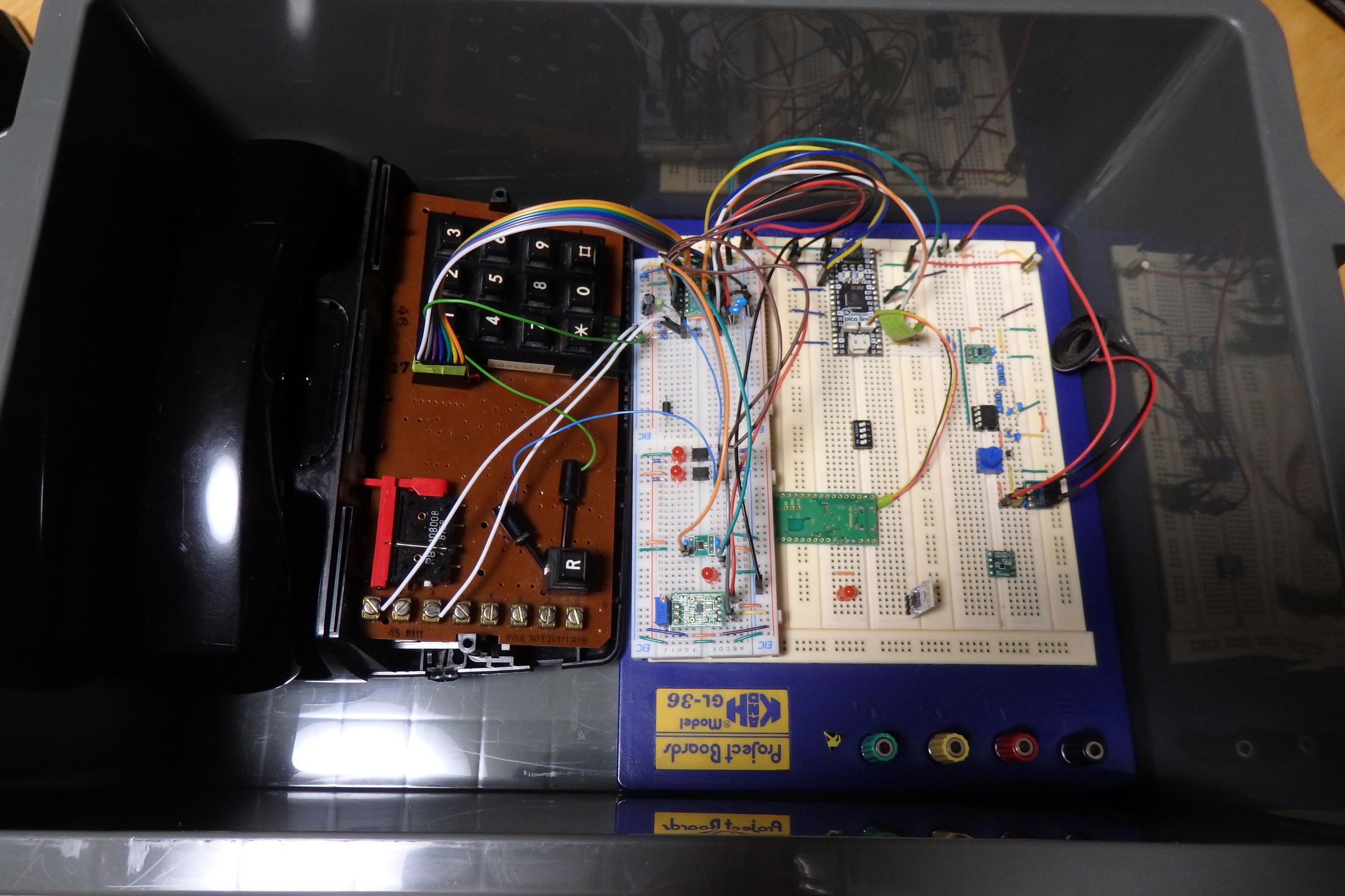
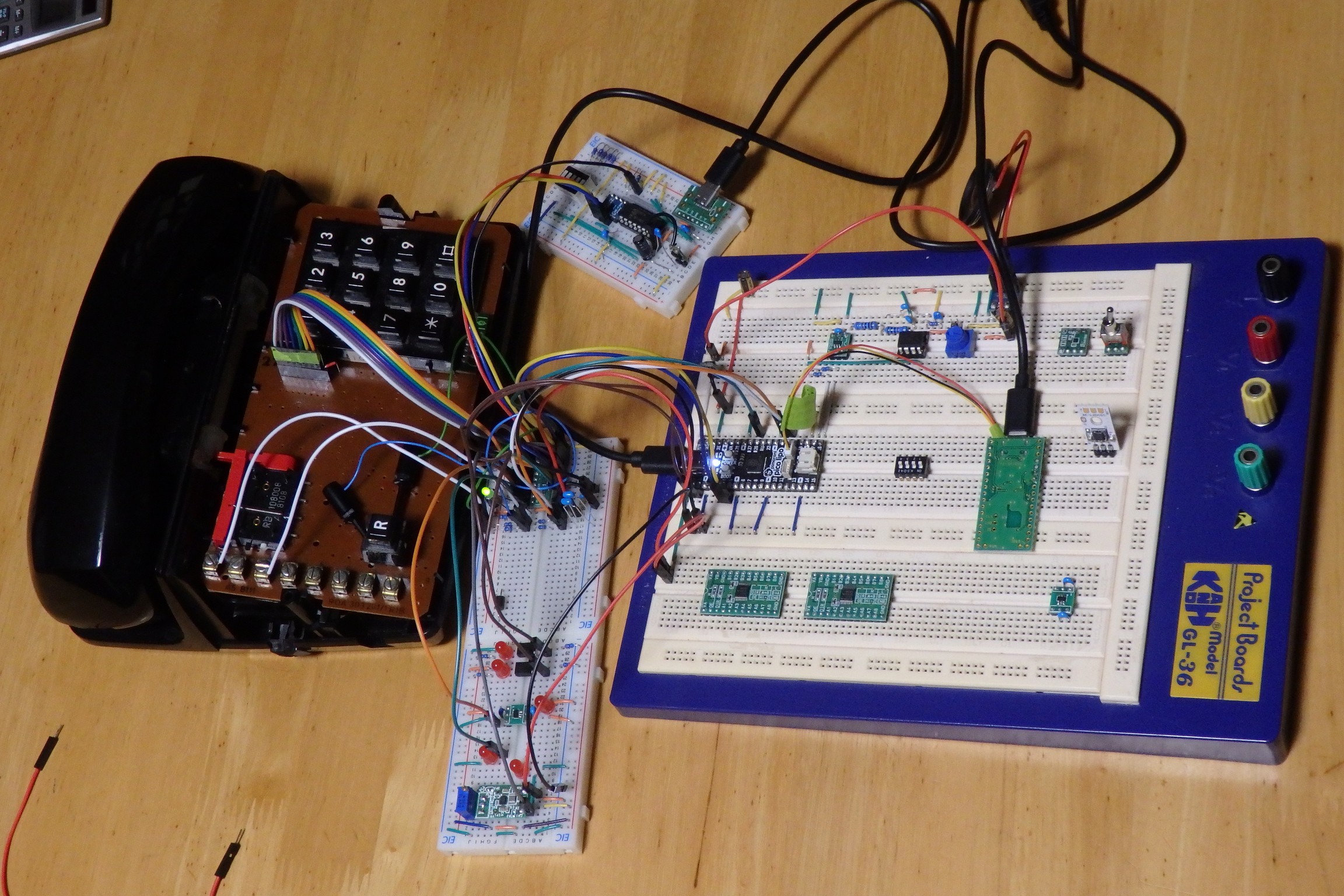
The Diavox Project "Old phone cellphone"
Where to start?
The scope of the project is rather large so it is divided into sub-projects and their individual tasks. Some have dependencies which have to be completed first.
| Sub-project | Status |
|---|---|
| Debug probe | Completed ✓ |
| Rust programming toolchain | Completed ✓ |
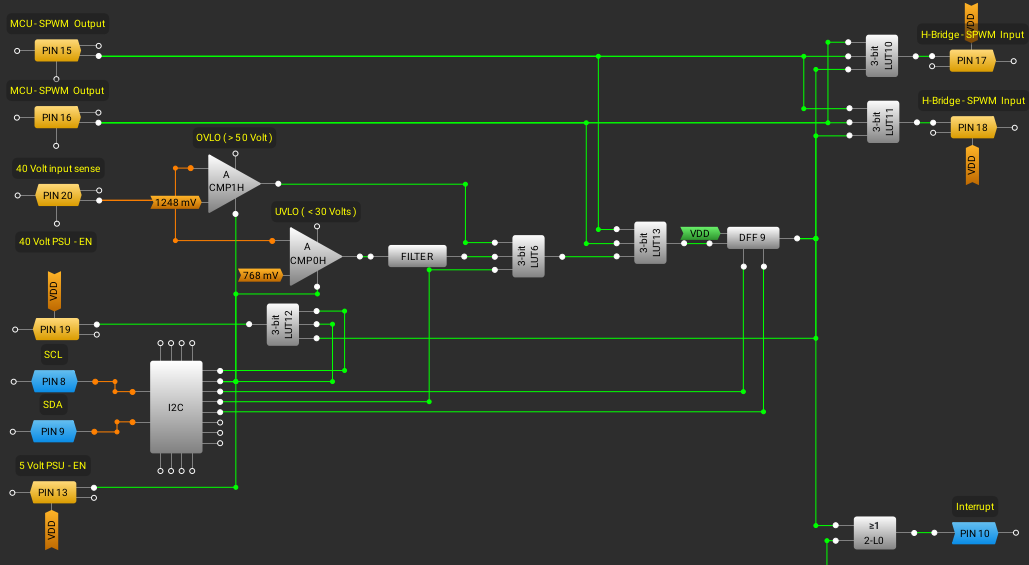
| Bell ringer | Underway |
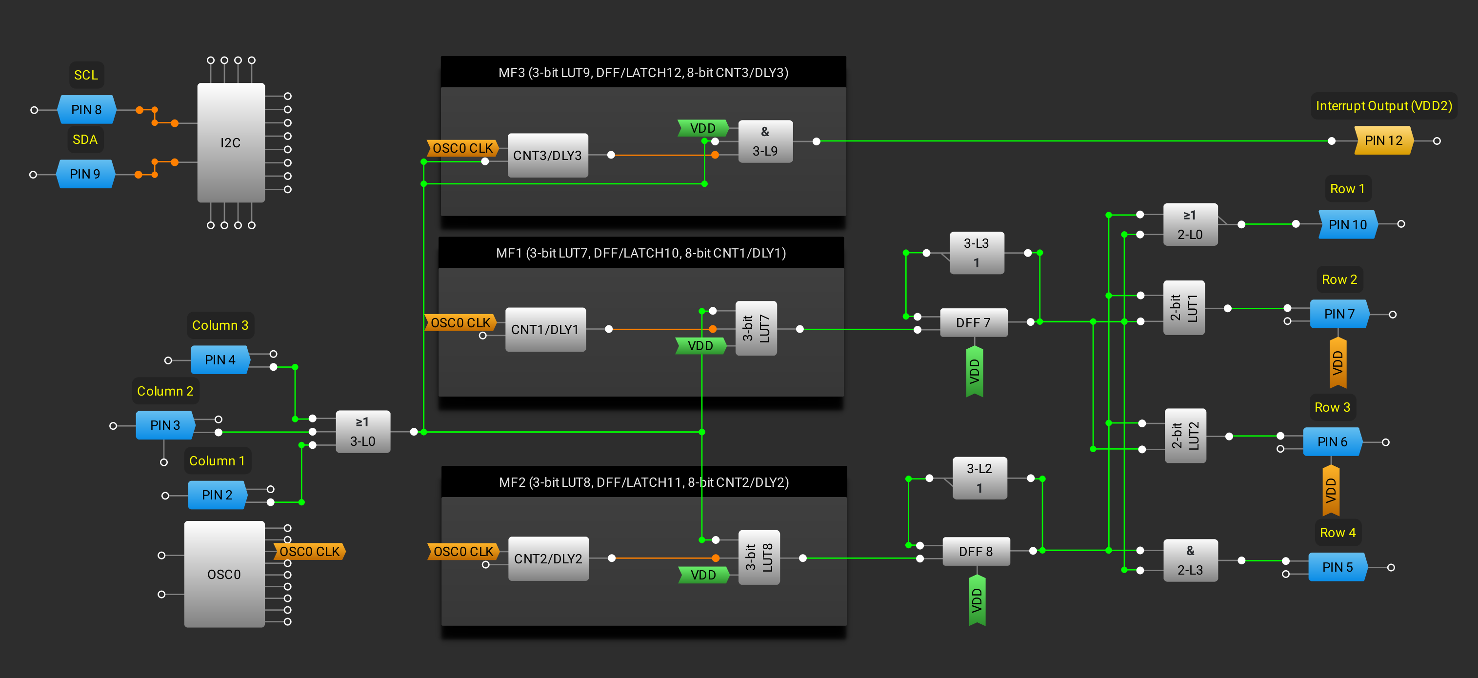
| Keypad matrix scanning | Completed ✓ |
| DTMF keytone generation | Completed ✓ |
| Codec breakout PCB | Started |
| LTE Modem | Not Started |
| Handset speaker and microphone | Not Started |
| Connecting everything together | Not Started |
| Power supply | Not Started |
| Programmming | Started |
| Post-prototype refinement | Not Started |


Interesting idea. Is the DTMF tone generation to make it sound like the old days? AFAIK that's not how numbers are "dialed" with mobile phones. Although some automated response systems will want DTMF tones during a call for responses.
Also speed dial storage could be considered. Punching 10+ digit numbers for frequently called people will get old.