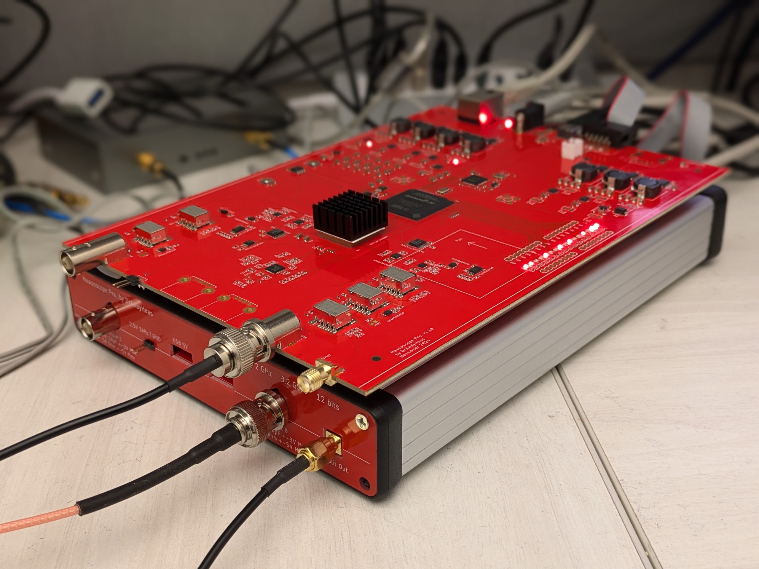
-
Anti-aliasing
12/15/2024 at 03:56 • 0 commentsThe Haasoscope Pro can be used in several configurations, leading to three different per-channel sample rates:
- One device with both channels active, so 1.6 GS/s on each channel
- One device with just one channel active, so 3.2 GS/s on one channel
- Two devices with just one channel active total (oversampling), so 6.4 GS/s on one channel
(You also could have two devices with one channel active on each, or two devices with two channels active on each, or two devices with one channel active on one and two channels active on the other, or more than two devices with all sorts of combinations! But any channel will still be at one of the three sample rates mentioned above.)
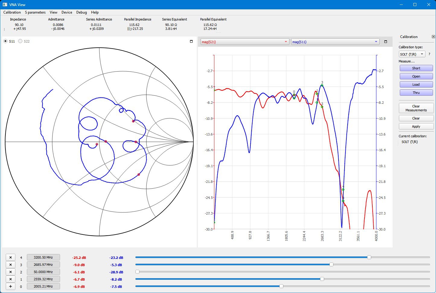
However, the analog bandwidth of each channel will still be at least 2 GHz in all these cases. In fact, it's only down by ~-3 dB by 2.5 GHz, and significant signal ~-10 dB still gets through by 3.5 GHz. This leads to a problem called aliasing, whenever there is analog signal coming in with a frequency greater than half of the sampling rate. For instance, even for the highest sampling rate, 6.4 GS/s, we would ideally have no frequencies entering the ADC above 3.2 GHz. But unless we do something, the signal is only down by ~-6 dB at 3.2 GHz. And things would be much worse even for the lower sampling rates.
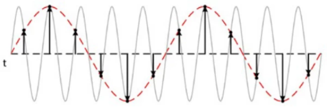
The effect is that those higher frequencies would look like lower frequencies in the ADC output, e.g. a sine wave with a frequency of 3.3 GHz would look like a 0.1 GHz (100 MHz) sine wave when sampled at 6.4 GS/s. That is inaccurate and confusing! Here's an example of an 800 kHz wave being sampled at 1000 kHz, and the result looking like 200 kHz.

To combat this issue, we need a low-pass filter in front of the ADC to filter out higher frequencies. In fact, we'll need 3 different filters with different cutoff frequencies (0.8, 1.6, 3.2 GHz) to address the 3 different possible sampling rates we can have (1.6, 3.2, 6.4 GS/s). There are all sorts of filter designs out there with various pluses and minuses. Some filter types are really flat in the passband, but then suffer from a slower rolloff after the cutoff frequency, or vice versa. There's no perfect filter - you have to just pick the design that has properties which suit your application. I'm pretty sure you can spend a full year in graduate EE school just studying filter design!
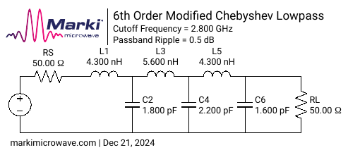
I chose the 6th order Modified Chebyshev filter with 0.5 dB ripple, because it has pretty fast rolloff and is pretty flat in the passband. Thanks to a plethora of free online design tools, designing the filter is trivial. Due to limited rolloff rate, we can't set the cutoff frequency to 3.2 GHz if we want strong suppression beyond 3.2 GHz. Setting the cutoff frequency a bit lower, like 2.8 GHz, gives the filter time to roll off. This is what the calculator gives:


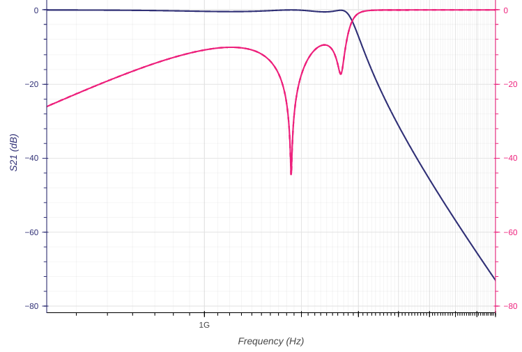
As you can see, the response is down ~-12 dB (a factor of 4) by 3.2 GHz, and is really flat until ~2.7 GHz. You could try a higher order filter, with more components, to get a faster rolloff, but then you also get a larger delay of the signal near the cutoff. This 6th order one has just ~100 fs of delay below ~2.3 GHz, which is OK for the targeted ~175 fs risetime of our 2 GHz system.
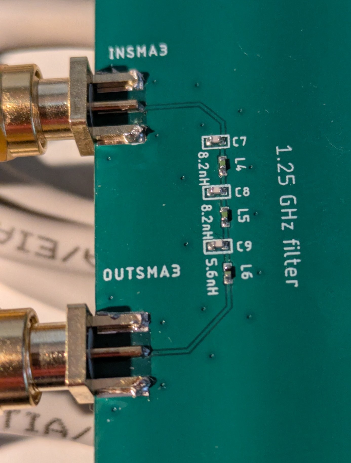
Well, that's the theory at least. Of course reality is a bit trickier, especially when dealing with single digits of nH's and pF's. Recall that a 1 mm trace has an inductance of ~1 nH, and an 0805 set of pads has close to ~1 pF of capacitance with a nearby ground plane - so parasitics are going to be significant here! This is what my little test circuit looks like:

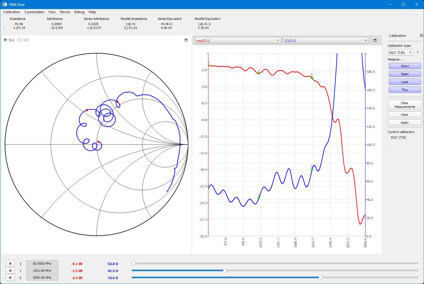
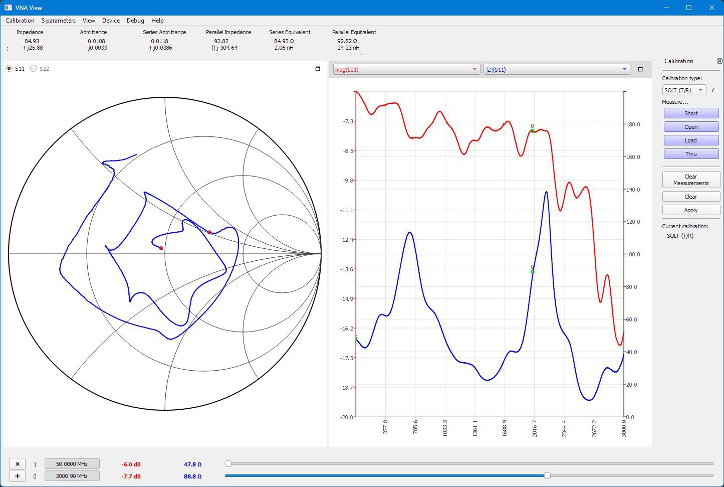
And here's how that board with a 2.5 GHz theoretical filter actually performs, as measured with the Nano VNA:

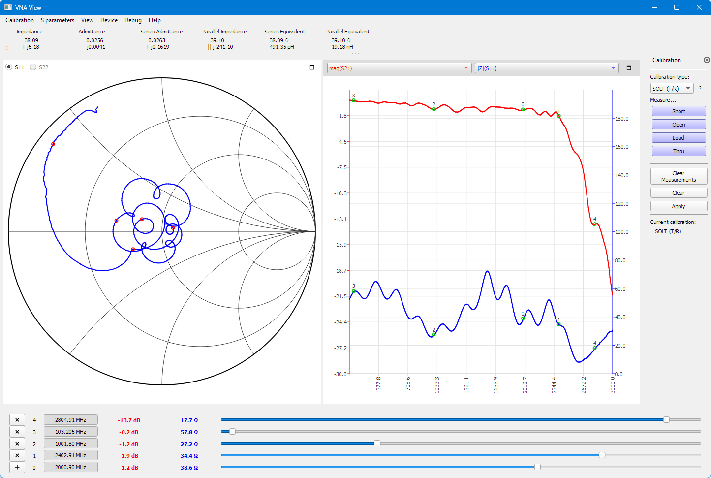
It starts to rolloff about 500 MHz low, so around 2 GHz, but it does have just ~0.5 dB of ripple in the passband, and it does rolloff at the right rate. We need a little tuning of the inductances and capacitances, to account for the parasitics. Here's what it looks like with 3.9, 5.1, 3.9 nH, and 1.2, 1.5, 1.0 pF (i.e. about 0.4 nH and 0.6 pf less per component):

That looks pretty good! It's flat up to ~2.4 GHz and then drops off nicely. Hopefully it'll still work well on the real board, since the parasitic capacitance will be a bit higher on the 10-layer Haasoscope Pro board with a GND plane just 0.1 mm away, rather than 0.2 mm away like on this 4-layer test board.
Update: after some tuning, it looks pretty good still on the final 10-layer board:

-
Oversampling
12/13/2024 at 04:27 • 0 commentsEach Haasoscope Pro can sample up to 3.2 GS/s on a single 50 Ohm input. But to take advantage of the 2 GHz of analog bandwidth, we need at least 4 GS/s according to the sampling theorem and of course more is better. Fortunately, Haasoscopes are meant to be synchronized, and by combining two Haasoscope Pro's we can get double the sample rate, 6.4 GS/s. The idea of oversampling is just that the samples from one ADC are interleaved in time with the samples from the other. For example, if ADC1 is sampling at times 0ns, 1ns, 2ns, etc. then ADC2 samples the same signal at times 0.5ns, 1.5ns, 2.5ns, etc. Sounds easy, but we need to get the analog signal into the second ADC while maintaining sufficient bandwidth. And we also have to sample the signal in both ADCs at sufficiently accurate times, with sufficiently small jitter.
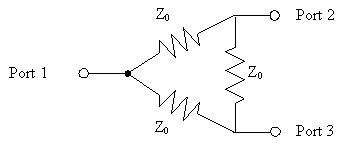
To get the analog input signal split off into the second Haasoscope Pro, we use a resistive power splitter. The input at port 1 on the left gets split using 3 resistors into the two ports on the right. The resistors just need to have resistance equal to the characteristic impedance of the inputs and outputs, which is 50 Ohm for us.

Actually, the input and outputs are all symmetric as you can see, so any one of them talks to the other two. This works great up to very large frequencies, limited only by the parasitic capacitances and inductance of the resistors. The outputs will each be 6 dB smaller in voltage than the input, so 1/4 of the input power. (Half of the power is wasted as heat in the resistors.) One output is sent to the ADC on the first board, and the second output is sent out to an SMA connector on the front panel. An external SMA to BNC 50 Ohm coaxial cable can then be used to get the signal to the input of the second Haasoscope Pro for sampling by its ADC.

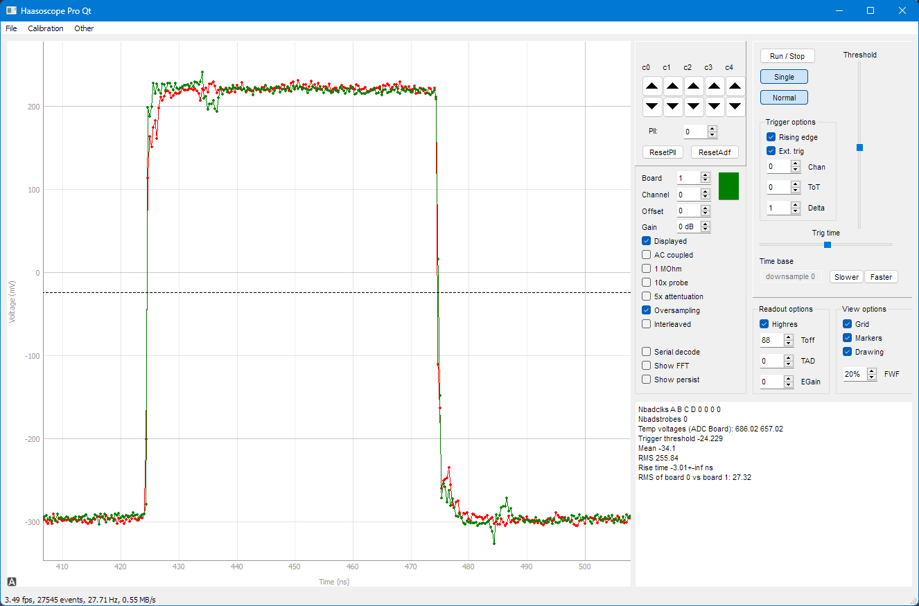
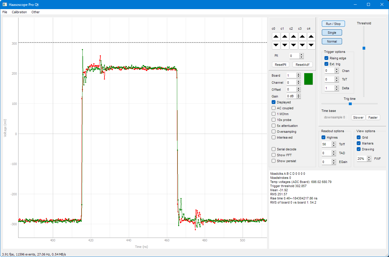
That basically works, as shown just below. The green is a signal sampled by the first board, and the red is the same signal triggered by the first board but sampled by the second board. Looks pretty good, but not great. The signal has degraded a bit by the time it gets to the second board, particularly at higher frequencies (close the sharp rising edge).

This is expected, since it had to go down more PCB traces, and through an extra SMA and BNC connector, and through a cable, all of which have more signal loss at higher frequencies. In fact, a NanoVNA V2 PLUS4 was used to test the frequency response of the whole splitting path. It's indeed down by about 2dB at 2 GHz compared to at low frequencies.

To recover these losses and make the two signals seen by the two units more similar, we need to allow more higher frequency signal through the splitter for the second output. The idea is to decrease the impedance of its nominally 50 Ohm resistor by adding a capacitance in parallel, whose impedance of course decreases as frequency increases. The relevant frequency where the parallel path will start to significantly impact the impedance is about 1/2piRC or about 400 MHz for 15pF, given the 25 Ohm relevant here in the splitter leg. The result looks like this (the red and green got switched I think):

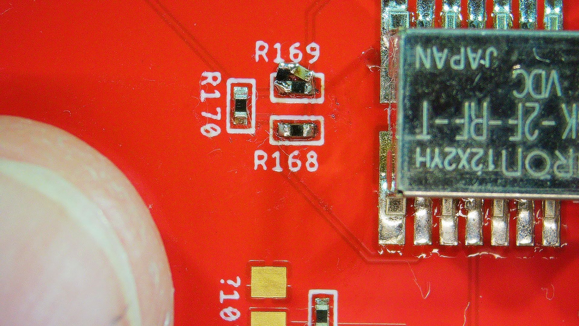
The green definitely is boosted at high frequency, but the issue is that the impedance now goes to zero at high frequency, so there's a big spike on the rising edge. What we need is some additional resistance on that parallel capacitor path, so when the impedance of the capacitor goes to zero, there's still the impedance of the resistor in series with it. This is what those 0402 components look like, with the tip of my finger for scale, hacked onto the board.
This is what it looks like with 15pF in series with 15 Ohm on the parallel path:

Much better! But it still dips down a little. Here's 27pF in series with 27 Ohm:

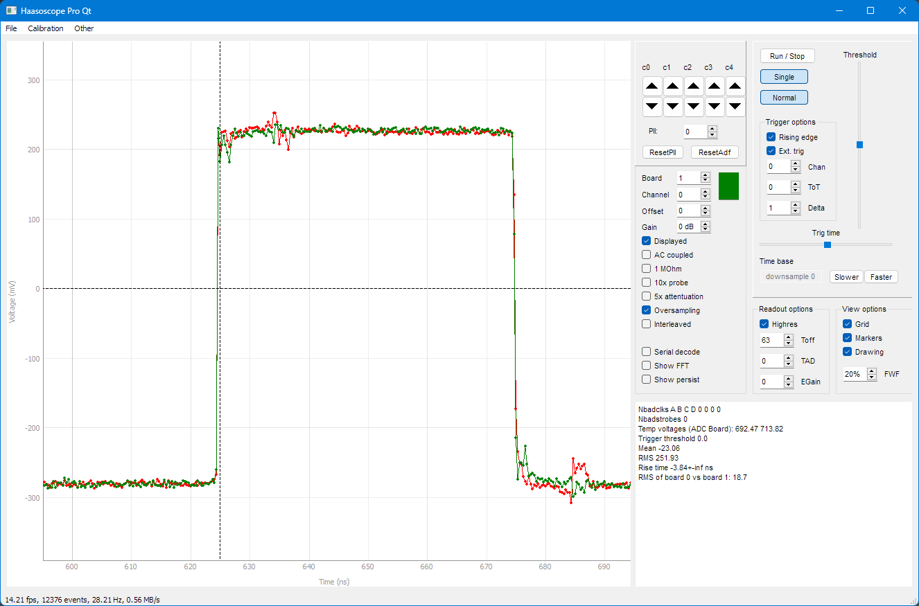
There's still a small remaining issue, which is the small reflection on the first board's signal (red), just after the rising (or falling) edge. That's coming from a small impedance mismatch between the cable and the SMA / BNC connectors I think. It moves in time depending on the length of the cable. Adjusting the termination impedance of the single-ended to differential amplifier, the LMH5401, from 357 Ohm (as recommended in the datasheet) to 220 Ohm seems to help. Here's what it looks like, after also changing to 16pF in series with 47 Ohm:

I am sticking with that for now. But before interleaving, we have to shift the sample time for the second board by 1/2 a sample period, which is just 0.5 * 1/3.2GHz = 156.25 ps. Fortunately, our fantastic ADC allows us to shift (delay) the sample time digitally via SPI commands, up to 289 ps, with a resolution of 19 fs!
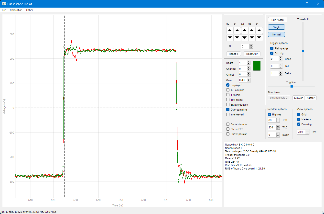
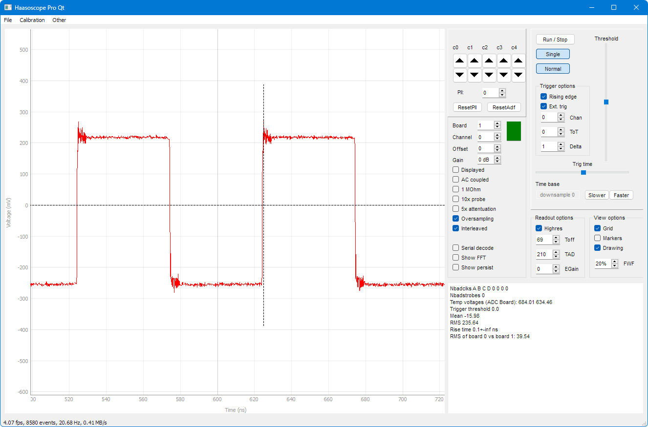
We're now ready to interleave the samples from the two boards, in software, which gives these results with 6.4 GS/s:

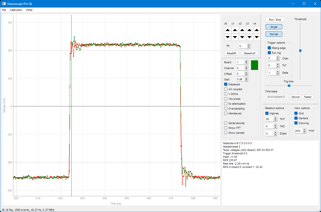
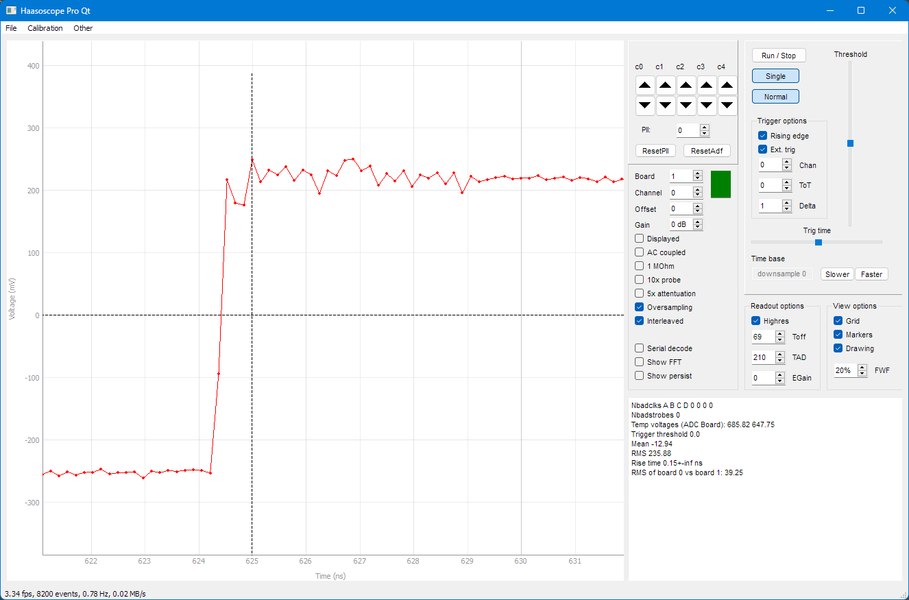
That's a lot of samples on a 10 MHz square wave, and very sharp rising edges. Here's a zoom in of one of those edges:

There is still a small amount of high frequency loss on the rising edge, but it's pretty darn good. And that cable/connector impedance mismatch reflection gives a bit of difference between the two boards, leading to the alternating sample "noise" on the plateau after the rising edge. But this performance is still astonishing. We expect at best a risetime of 0.35/2GHz = 175 ps for a bandwidth of 2 GHz, and we are getting at least that. This particular edge, from a pulse generator with a risetime of ~40 ps, had a measured risetime of 150 ps!
-
Overview of the firmware
12/08/2024 at 18:21 • 0 commentsThe firmware running on the Cyclone IV FPGA of the Haasoscope Pro is the central brains of the whole oscilloscope. Its key jobs are to:
- Control and monitor the behavior of the many ICs on the board such as DACs, amplifiers, the main ADC, etc. over SPI
- Collect and synchronize data coming from the main ADC, using 56 LVDS pairs
- Process the incoming ADC data, including triggering, downsampling (optionally ignoring some fraction of samples to decrease the effective sample rate), and buffering of the triggered data while waiting for readout
- Accept and respond to commands over USB via the FT232H chip, including sending out the buffered ADC data over USB
The firmware is written and compiled using the Altera Quartus IDE. The "lite" version is free, and runs on Windows or Linux. To get started, just open the Haasoscope Pro firmware project file, "HaasoscopePro/adc board firmware/coincidence.qpf".
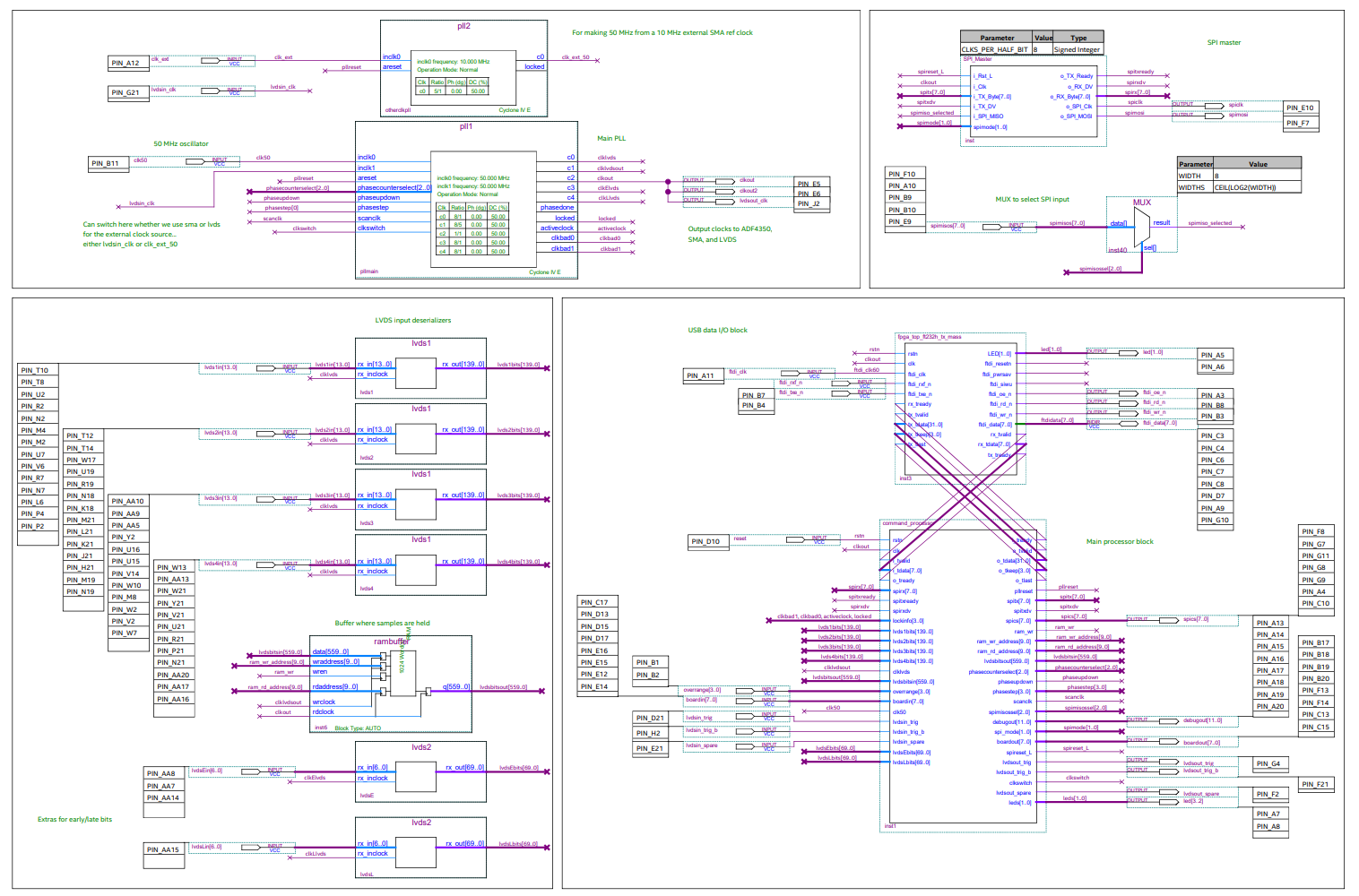
Here's an overview of the firmware structure, as seen in Quartus:

These are the basic building blocks:
- PLL block, top left, provides clocks for other blocks
- LVDS input blocks, below the PLL, handle LVDS inputs from the main ADC and output data to the main processor block
- Data buffer block, below the LVDS blocks
- SPI controller block, top right, handles SPI communication to/from various chips and the main processor block, and the SPI input MUX, below the SPI block, switches which SPI input is being listened to
- FT232H USB block, below the MUX, buffers and handles USB IO to/from the main processor block
- Main processor block, bottom right, is the main brains: receives and responds to commands from the USB block, handles main ADC data from the LVDS inputs, triggers on the ADC data, processes and buffers triggered ADC data
Let's now look at each block in a bit more detail.
PLL block
The PLL can take in either a 50 MHz clock from the board's 50 MHz crystal, or an external 50 MHz clock from LVDS (used for synchronizing multiple boards). Outputs tell the main processor block which of the two input clocks are available, which is actively being used, and whether the PLL is locked. An input, "clkswitch", is controlled by the main processor block and decides which clock input is active.
There are 5 clocks output from the PLL:
- c0 runs at 8*50 MHz = 400 MHz and tells the LVDS input blocks when to sample inputs. The LVDS inputs are DDR, so thus run at 800 MHz each, near the limit of the Cyclone IV.
- c1 runs at 8/5 * 50 MHz = 80 MHz and tells the main processor when to read from the LVDS input blocks. Each LVDS input block takes in 10 bits of serial data at 800 MHz and then outputs a single 10-bit wide block of data at 80 MHz. This de-serialization is key to allowing the FPGA to process the data, since the FPGA logic runs at a max clock rate of a few hundred MHz.
- c2 is a 50 MHz output copy of the input clock, but de-jittered by the PLL. It drives the main processor logic which interfaces to the USB block, outputs to the LVDS clock out for syncing other boards, and outputs to the ADF4350 PLL for making the 1600 MHz differential clock that drives the main ADC.
- c3 and c4 are also 400 MHz outputs that drive subsets of the LVDS inputs whose connections from the main ADC are either shorter or longer, respectively. The LVDS signals travel at about the speed of light / 2 in the board, since the dielectric of the FR4 is about 4, and it goes like the sqrt of the dielectric. So they travel at about 30cm/ns / 2 = 15 cm/ns. The shortest LVDS connection is about 2 cm and the longest is 6cm, so there's a 4 cm difference, or 4cm / 15cm/ns = ~0.3 ns max time difference. At 800 MHz, that's a sample every 1.25 ns. That's a significant enough difference that some of the inputs may not be sampled correctly if all are driven from the same clock. We could have tried to make all the LVDS connections more similar in length, by meandering the tracks, but this is a bit tricky for differential tracks while maintaining impedance (in Eagle), and the routing is already extremely dense. Instead we just drive the short, standard, and long tracks each on their own LVDS clock, c3, c0, and c4, respectively, and let the LVDS input blocks synchronize them. The outputs of the LVDS blocks are all read on the same clock, c1.
There is an interface to the PLL, connected to the main processor block, for dynamically adjusting the phase of each output clock. This is used to adjust the phase of each of those LVDS clocks, so all the LVDS inputs can be synced.
LVDS input blocks
We've mostly already discussed the LVDS blocks. There are 4 12-bit LVDS inputs, so 48 LVDS pairs coming from the main ADC, which is 3200 MHz of 12-bits data. There's also a clock and a strobe LVDS input for each of the 4 12-bit LVDS busses, so 4*12+4*2=56 LVDS inputs total, each running at 800 MHz. I still find it amazing that an FPGA like this can process that much data, 44.8 Gb/s, for ~$75, using ~1W!
Data buffer block
The data buffer is an array of FPGA memory 1024 words long and 560 bits wide, that stores the processed ADC data before it's read out. (560 bits = 12 bits + clock + strobe for each of the 4 LVDS busses from the ADC, times 10 samples per c1 LVDS deserialized readout clock tick.) There's no external RAM on the board. Interfacing to that would require another huge number of LVDS connections in order to write the data to RAM fast enough to keep up with the ADC. Processed data from the main processor block (see below) is written by it into the data buffer. It's a circular buffer. Data is constantly being written every clock cycle into the buffer to a location that is incremented, and the current write location is wrapped back around to the beginning of the buffer when it reaches the end of the buffer. When a trigger occurs, the main processor stops writing into the buffer after a given number of clock ticks. This allows for B samples to exist in the buffer before the trigger and A samples after the trigger, where A+B=1024. The division between A and B is set by the "trigger position" command via the software.
SPI controller block and SPI input MUX
The SPI block listens to commands from the main processor block and creates SPI commands to send to target devices on the board. It's based on spi-master by Nandland. Then there's an input MUX to select which device we want to receive SPI data from. All higher level SPI sequencing, which just to send, read, etc., is handled in the main processor block.
FT232H USB interface block
The USB interface block communicates between the main processor block and the FT232H chip that talks to the software over USB. It is based on FPGA-ftdi245fifo by WangXuan95. Bytes received from the software go into a FIFO in the USB interface block, which then can be read by the main processor block. Bytes sent from the main processor block go into another FIFO in the USB interface block, which then are sent out over USB to the software. The USB block has its own 60 MHz clock, generated by the FT232H chip from an external 12 MHz crystal on the board, to handle the physical layer USB communications.
Main processor block
The main processor block is where most of the real logic and processing occurs. The file is "command_processor.v". There are three main sections.
The first section takes the input LVDS data from the main ADC and creates the "samples" that will be stored into the data buffer. These samples may need to be slower than those being provided by the ADC. For instance, the ADC is sampling at 1600 MHz on two channels, but we may want to see a longer length of time in our data buffer, i.e. we may want a longer time base, say 1 ms / division. To do that, we need to ignore almost all of the incoming samples, but just keep 1 out of every N samples... enough to fill the data buffer after 10 ms (assuming 10 divisions). This is called downsampling. It gets a little complicated - actually super annoyingly complicated (I banged my head on the wall for many hours to get it right!) - because the samples are coming in 40 at a time in each clock tick, thanks to the LVDS 10x deserialization and the 4x LVDS busses which are interleaved (or 2x if we are in two-channel mode).
The next section handles triggering. We have rising edge and falling edge triggers, as well as external triggers coming from another board or external input. More triggers may be added of course. When a trigger occurs, we have to record which of the 40 samples of the clock tick actually crossed the trigger threshold, and also at which position we were writing into the data buffer. We'll need to know these for the data readout later and for correctly positioning the data on the screen in the software. Once a trigger occurs, we freeze the writing into the data buffer and wait for readout.
The last section runs on the 50 MHz clock, not the 80 MHz LVDS buffer read clock used for the above sections. It takes in commands from the USB interface block, possibly does some things, and then responds to the USB interface block by sending it data. The commands come in as 8-byte words. The first byte determines the type of command. For instance, if the first byte is 0 it sends back the data buffer, if it's 1 it sets channel and trigger types and sends back trigger info for the last event, if it's 2 it sends back the firmware version or other info, 3 is for an SPI command, etc. The other 7 bytes in the command can be used as parameters for the command, if needed.
Timing
Lastly, the firmware would be nothing without detailed timing constraints. They are in the file "coincidence.sdc". These tell the Quartus compiler what must happen by when. Quartus then attempts to "fit" a firmware which satisfies these constraints, by placing logic in the FPGA at locations such that routing delays are small enough so that things happen by when they need to.
First, the clocks are defined. Then clock groups are defined which tell Quartus which clocks are unrelated to each other. For instance, the clocks based on the 50 MHz crystal input and the 50 MHz external LVDS input clock are not related since only one set is active at any given time. The 60 MHz USB clock is also not related since it is used by a separate block only.
Next we ignore some routing paths which are known to be erroneously flagged by Quartus as warnings. It's important to let Quartus know these are not really problems so it doesn't ruin other routing trying to solve them.
Last, and maybe most importantly, we set the timing constraints for each external input and output. These are saying how early or late each IO pin can be compared to the others. LVDS inputs are of course critical to time accurately, as well as the signals interfacing with the FT232H USB chip. SPI signals need be less strongly constrained, etc. Only after properly defining these constraints does the resulting firmware behave as we like. And we can be pretty sure it will perform correctly by checking the Timing Report in Quartus which will tell us if the constraints could be satisfied, and if not where not and by how much.
Results
Quartus provides a nice summary of FPGA usage:
Total logic elements 11,564 / 28,848 ( 40 % )
Total registers 4107
Total pins 228 / 329 ( 69 % )
Total memory bits 592,000 / 608,256 ( 97 % )
Embedded Multiplier 9-bit elements 0 / 132 ( 0 % )
Total PLLs 1 / 4 ( 25 % )We are only using about half of the available logic, though closing timing constraints gets harder once more of the FPGA is used, depending on what that logic needs to access. There's still over 100 IO pins free, so more IO could be added to the board design, though routing is starting to get tricky. We're using nearly all the FPGA memory for the data buffer (and a little for the USB FIFOs) - 1024*40 12-bit samples just fits! We're not using any of the DSP resources - they could be used for filtering? FFT in firmware? And finally, we do have lots more clock resources that could be made use of. It's pretty amazing how much more could still be added to the design, given how much we're doing already. And this is only a medium-sized Cyclone IV from 2009! Imagine what the newly released Altera Agilex FPGAs will be capable of!
-
Syncing units
12/08/2024 at 18:19 • 0 commentsHaasoscopes can be connected together, to either increase the number of channels, or to oversample an analog input to double the sample rate. (We'll have a separate log post about oversampling soon.) The first step in making this possible is to synchronize the clocks between multiple units. This is essential for sampling at the same instant, and also makes it easier to communicate other data between units since inputs can be sampled synchronously on the same clock edges. We'll also need to send trigger signals between units, in both directions, since when either unit triggers we want the other unit(s) to also trigger.

Simple wires won't work because the signals are high speed. The clock we want to send, for instance, is 50 MHz. And the trigger signal edges need to be ~ns risetime with ~ps jitter. We need controlled impedance transmission lines, so we're not broadcasting like a 50 MHz radio station and receiving massive RF interference. We could use coaxial cables, like SMA, but we'd need at least 3 of them. The connectors and cables aren't cheap, they're bulky, and they get messy.
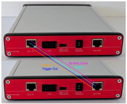
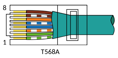
Instead, all these signals are sent over a single Ethernet cable, which offers 4 LVDS pairs and is cheap, ubiquitous, and sturdy. Note, we're not using Ethernet packets or anything at all, just the connectors and the cable. Technically, a standard Ethernet cable is RJ45 jack with an 8P8C connector, as shown here.

The FPGA on the Haasoscope Pro can easily be programmed to send and receive these LVDS signals as standard IO's. The only extra thing needed is a single 100 Ohm resistor at the receive end of the cable to terminate the signal, which we place on the bottom of the board directly under the FPGA, connected with vias, just like for the termination resistors for the ADC LVDS inputs.
We can connect as many Haasoscope Pro's as we want, by daisy chaining them together, since each Haasoscope Pro has a Sync In and a Sync Out port. We do need to figure out which unit is where in the chain, though. To determine the order, we first find the one unit which has no good clock coming into its Sync In port, by looping through all the connected units and asking each of them if they have a lock on their external clock input. Once we know the first unit, we attempt to find the next one in the chain, the one it's connected to. We make use of the 4th LVDS pair in the cable, the "spare LVDS". We set it high on the output of the first in the chain, then see which of the other units sees a high value on their spare LVDS input. (All other spare LVDS outputs are set low by default.) Once we know the second unit in the chain, we can then find the third in the chain by repeating this trick with spare LVDS signals.
-
Making a case
12/08/2024 at 18:18 • 0 commentsA serious instrument like the Haasoscope Pro needs a good enclosure, to protect the expensive things inside, keep the board from shorting out on other things on your desk, and keep out RF interference. Plus it just looks good and professional!
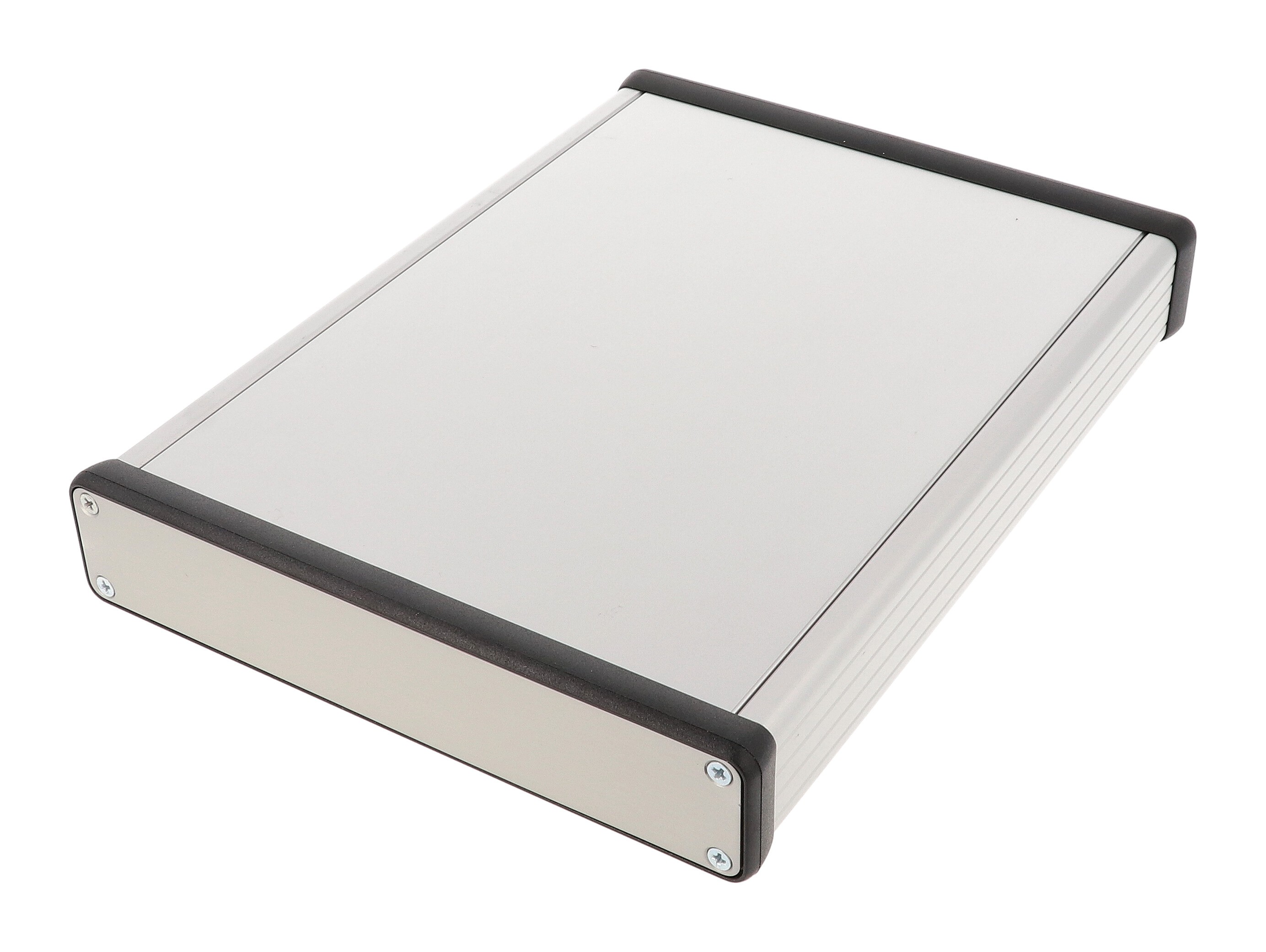
I decided to go with an extruded aluminum enclosure. It's cheap, easy, works great, and looks pretty good. This one from Hammond is the perfect size for the project, and only ~$30.

There's nice rails on the inside between which you can slide a PCB (or even multiple PCBs). It took a little experimentation to find just the right size to make the PCB so it fits snug.
The only work is in getting just the right openings in the front and back panels so the connectors fit. At first I thought about having aluminum panels laser cut. But how do you get the text printed on for the labels? A much easier way is to just to make PCBs for the panels! They can have whatever shaped cutouts you want, nice text printed on, and even come in cool colors. You could even have active components on the panels, like LEDs, but this would require some connectors and cables for power and communication with the main board.

To retain the RF shielding, a GND plane is added on the back of each panel.
One last worry is heat. The Haasoscope Pro uses about 6W while it's active, about 3W of which is coming from the ADC, 1W from the FPGA, 1W from amplifiers and other random stuff, and 1W from power supply inefficiencies. The aluminum enclosure can easily dissipate this amount of power with minimal temperature rise inside, thanks to its large surface area. But 20x20x10mm aluminum heatsinks are added on the ADC and FPGA with thermal tape, since they're small and generate most of the heat. A small 40x40x10mm 5V 60mA fan is also glued to the inside of the top of the case and blows onto the ADC (and slightly on the FPGA) when the unit is active.
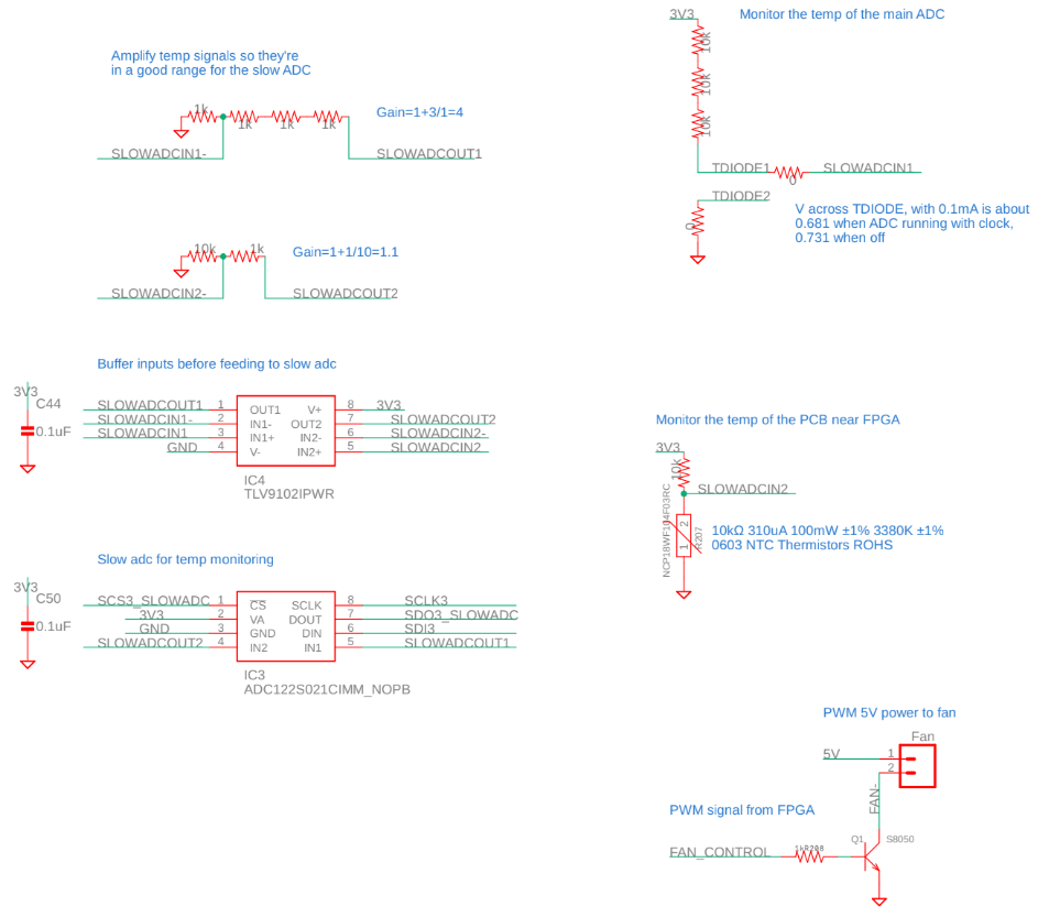
Temperature monitoring is done in two places. The ADC has an internal temperature diode - the voltage across it, measured across two of the ADC pins, goes from about 0.73V when off, to about 0.68V when running, when in series with a 33k resistor. There's also an NTC thermistor on board, which measures the ambient air temperature on the board near the FPGA. These two sensors get put into a slow dual op-amp and slow dual-channel ADC, which gets read out over SPI by the FPGA.

-
Walkthrough of the front-end design
12/01/2024 at 20:07 • 0 commentsWhen you hear "2 GHz oscilloscope", you might rightly wonder what kind of analog wizardry can possibly achieve such crazy bandwidth. Well, as you'll see, there was some care involved, but the real key was just to use some incredible components. In particular, the LMH5401 is a preamplifier with 8 GHz of gain bandwidth product that somehow only costs ~$10. We use it as a 4x gain, single-ended to differential amplifier. Then following that is the LMH6401, a 4.5 GHz bandwidth variable gain amplifier that somehow only costs ~$15. We use it to vary the gain by an extra factor of between -6 to 26 dB (~0.5x to ~20x), in 32 steps. Just using those two components, we basically have a 2 GHz front-end. The rest is just bells and whistles.
The front-end is basically all 50 Ohm (or 100 Ohm differential) impedance. 1M Ohm input impedance is accepted, but, as you'll see below, it is immediately turned into a 50 Ohm signal and then handled just like a 50 Ohm input.
Let's take a look at the schematics. The first page is the "pre-input" part. A single-ended BNC signal comes in, and a 50 Ohm single-ended signal comes out, which will go to the LMH5401 preamplifier on the next page. Along the way, we are handling the splitting out of an analog input for oversampling, switchable 50/1M Ohm impedance, switchable 5x attenuation to increase the dynamic range, and AC/DC input coupling. The main goal here is to accomplish these functions without ruining the 2 GHz bandwidth before we get to the fancy preamplifier on the next page.

We do have to be careful about the BNC input itself. Connectors are easy places to destroy bandwidth. Some BNC connectors only have 500 MHz or 1 GHz of bandwidth! We use Molex 73100-0105 BNC connectors, rated to 2 GHz, but I've tested them to 3 GHz and they show minimal losses (<1 dB).
Next is a stage which can optionally split out half the signal to an SMA output on the front, so you can send it to a second Haasoscope Pro for oversampling. This is only on channel 1, since if you're bothering to oversample the signal, you're going to be using the ADC in single channel mode to first get the full 3.2 GS/s for the channel. The splitting is done by a simple resistive divider in the Delta configuration. It maintains the 50 Ohm impedance of the signal along both paths. We're assuming that the signal is 50 Ohm here, because only 50 Ohm has 2 GHz bandwidth and would require oversampling. Half of the signal is lost to heat, but that's OK, we have amplifiers afterwards.
This, and other options, are switched on or off by a relay. But not just any relay - most will only have a few hundred MHz of bandwidth. We need special "RF relays". Here I settled on the Omron G6K-2F-RF-T, which is rated to 3 GHz, but really starts to degrade significantly after 2 GHz. But that's good enough for us here, and already it's ~$10 each. Better relays are available, but can easily be ~$100 each! They're DPDT relays, so it's easy to route signals either on one path or another path, since there's an "input" and an "output" switched simultaneously. If the relay is off, the signal just goes straight through on a 50 Ohm wire to the output. If the relay is on, the signal goes into the splitter and half of it goes to the output.
The next stage allows for switching to accepting 1M Ohm input impedance, for using standard 10x passive probes. These probes inherently don't have large bandwidth - the ones I usually use, the Rigol PVP2350 have 350 MHz of bandwidth, and the most you're likely to get from any passive probe is about 500 MHz. This is far from 2 GHz, so why bother with 1M Ohm impedance at all? Well, for one, some people just like to use 10x passive probes and don't care about the bandwidth. Second, if we're in two channel mode for the ADC, we have 1.6 GS/s per channel, and that's not such overkill for 500 or even 350 MHz of bandwidth.
The goal here is to deal with 1M Ohm input impedance, but then immediately turn it into a 50 Ohm signal, for processing like a 50 Ohm input. This lets us reuse the same magical high bandwidth 50 Ohm amplifiers we use for a 50 Ohm input. We "only" need to maintain ~500 MHz of bandwidth here, since the passive probes won't have more than that anyway. Here we make use of another fantastic chip, the OPA859 op-amp, with up to 1.8 GHz of bandwidth, somehow for only ~$3. At 2 Vpp, the bandwidth is down to 400 MHz, but that's still pretty much good enough. And importantly, the inputs are CMOS MOSFET inputs, meaning they are crazy high impedance, like 1G Ohm, with just 10 pA of input bias current. That means we can put a 1M Ohm input into it, and not have the amplifier itself affect the input signal.
A 1M Ohm input resistor from signal to GND sets the input impedance. We also want the input capacitance to be ~10-15 pF, which is what is expected by passive probes and standard for oscilloscope 1M Ohm inputs. The tuning screw on the probe can adjust the compensation, within a range, to account for varying oscilloscope input capacitance. I've found that the parasitic capacitance of the Haasoscope Pro input path, from the BNC input connector, the board traces, the component pads, the buffer amp, etc. seems to be about 10 pF already, so although the pads for an extra capacitor are there on the board, I don't add one at the moment. We use the op-amp as a simple unity-gain non-inverting buffer, and a 47 Ohm resistor is put on the output to make the total output impedance close to 50 Ohm.
The following stage is the switchable 5x attenuator, for increasing the dynamic range. It is 50 Ohm impedance, since everything is 50 Ohms at this point. It's a simple resistive pi-attenuator. This nifty calculator can tell you the two resistor values to use to get the desired attenuation while maintaining 50 Ohm impedance.
The final stage is AC/DC switching, which we do basically like all oscilloscopes do. A capacitor does the DC blocking, letting through only signals less than 1/2piRC. For us, R is 50 Ohm, so C needs to be as big as possible - we use 1 uF, giving a ~3 kHz cutoff. DC signals are let through by a photo-MOSFET when it is on. We need to make sure it doesn't add capacitance and ruin bandwidth though, so the TLP3475 is used. We could have used another relay here, but the photo-MOSFET is only $3, vs $10 for the relay, and there's two channels, so $14/board saved, plus less signal degradation and less board space. We also need to make sure the capacitor doesn't add significant impedance, something we don't usually worry about - but at some large frequency every capacitor becomes an inductor, past its "self-resonant" frequency. Fortunately, Samsung provides data on their capacitors, and for the one we use, it is indeed an inductor at 2 GHz (with a self-resonant frequency around 10 MHz!), but its impedance is only ~1.5 Ohm at 2 GHz, so not significant compared to 50 Ohm.
The second page is the "input" part. It takes in the 50 Ohm single-ended signal from the pre-input stage and puts out a 100 Ohm differential signal for the ADC. We already talked about the magic of these two parts, the LMH5401 and LMH6401 at the beginning of the post. Just follow the datasheets and they work. One detail is that I'm still optimizing the "termination resistor", the 357 Ohm one on OUTPATHMAIN. It sets the overall input impedance of the amplifier, and it seems like it's not quite 50 Ohms at the moment with 357 Ohm, despite saying it should be in the datasheet. Maybe my parasitic capacitances and/or inductances are a bit different than on their evaluation board? I'm working now on tuning it.

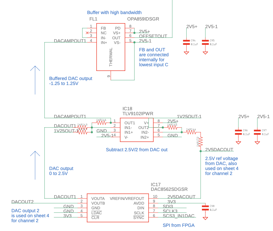
Along the way, we also apply an analog DC offset to the input signal. It goes to the "positive" input of the LMH5401 preamplifier. A dual output 16-bit DAC provides the settable offset voltage, which then goes through a low-bandwidth jelly-bean op-amp to move it from 0-2.5 V to -1.25 to 1.25V, as well as buffer the output. Then that output is fed to another OPA859 high-bandwidth op-amp, since we need to provide constant, low, output impedance to the LMH5401 input from DC - 2 GHz. (Reduce BOM count wherever possible!)

That is all for the first of the two input channels. Pages 3 and 4 just repeat this for for the second channel, except that the analog splitting is only done for the first channel.
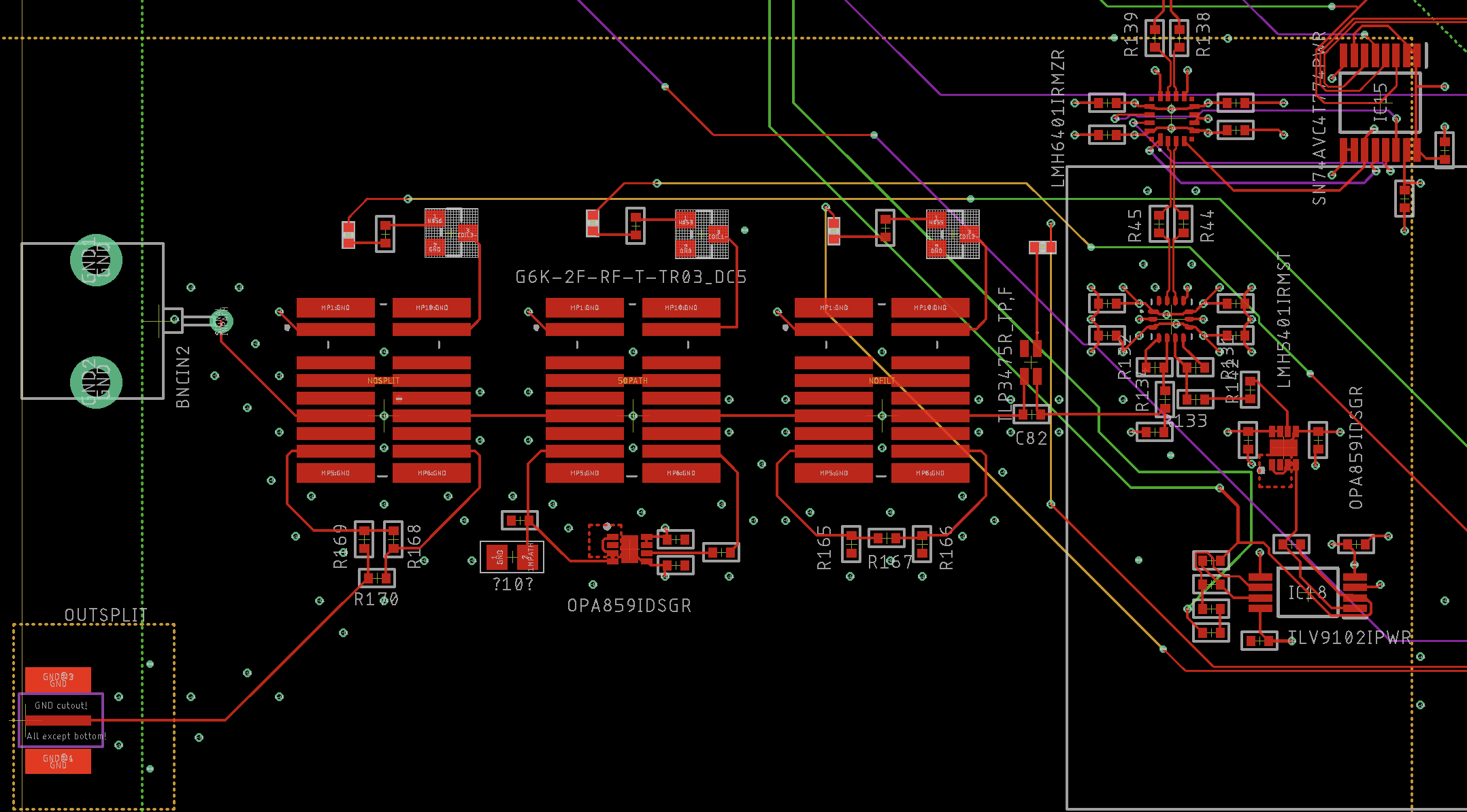
You can see the routing here, for the first channel. Starting from the BNC, all traces are 50 Ohm impedance, which means keeping them on the top of the board, layer 1 (red), and 0.16mm wide, given the 10 layer board stackup being used, with GND on layer 2 (not shown). There's also copious GND vias around the traces, at least every 1/10th of a wavelength at 2 GHz, which is about 30 cm * GHz (speed of light) / 2 GHz / 2 (sqrt of dielectric) / 10 = ~1 cm. And there's GND fill on the top layer (not shown), with 0.15mm between the GND fill and the traces, so nice coplanar waveguides.

And that's all there is to a 2 GHz front-end these days!
-
Early Development
11/28/2024 at 04:59 • 0 commentsIn July 2024, the kids were off to camp, and I was off from teaching for the summer. Relax? Vacation? No! Work day and night developing my own 2 GHz oscilloscope!
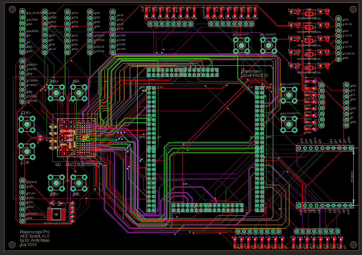
The first goal was just to talk to the ADC chip and get it to do something. This would convince me I could solder the BGA chip correctly in my little reflow oven reliably, power the chip correctly, and let me start playing around with it. I had to connect an FPGA to it, to talk to it over SPI and receive the LVDS signals it sends out containing the ADC data. So I wired it up to an FPGA dev board that I had experience using, based on a Cyclone IV FPGA. You can see in the pic below all the 2mm spaced pins where the dev board would connect to this new board hosting the ADC chip on the left. There were also SMA inputs for the (differential) clock signal and two analog input channels to the ADC. I also added lots of debug headers so I could probe every signal going into and out of the ADC, plus debug the power and signals from the FPGA. There's also two headers on the right for connecting a module based on the FTDI FT232H chip I had experience with for interfacing the FPGA to USB2.

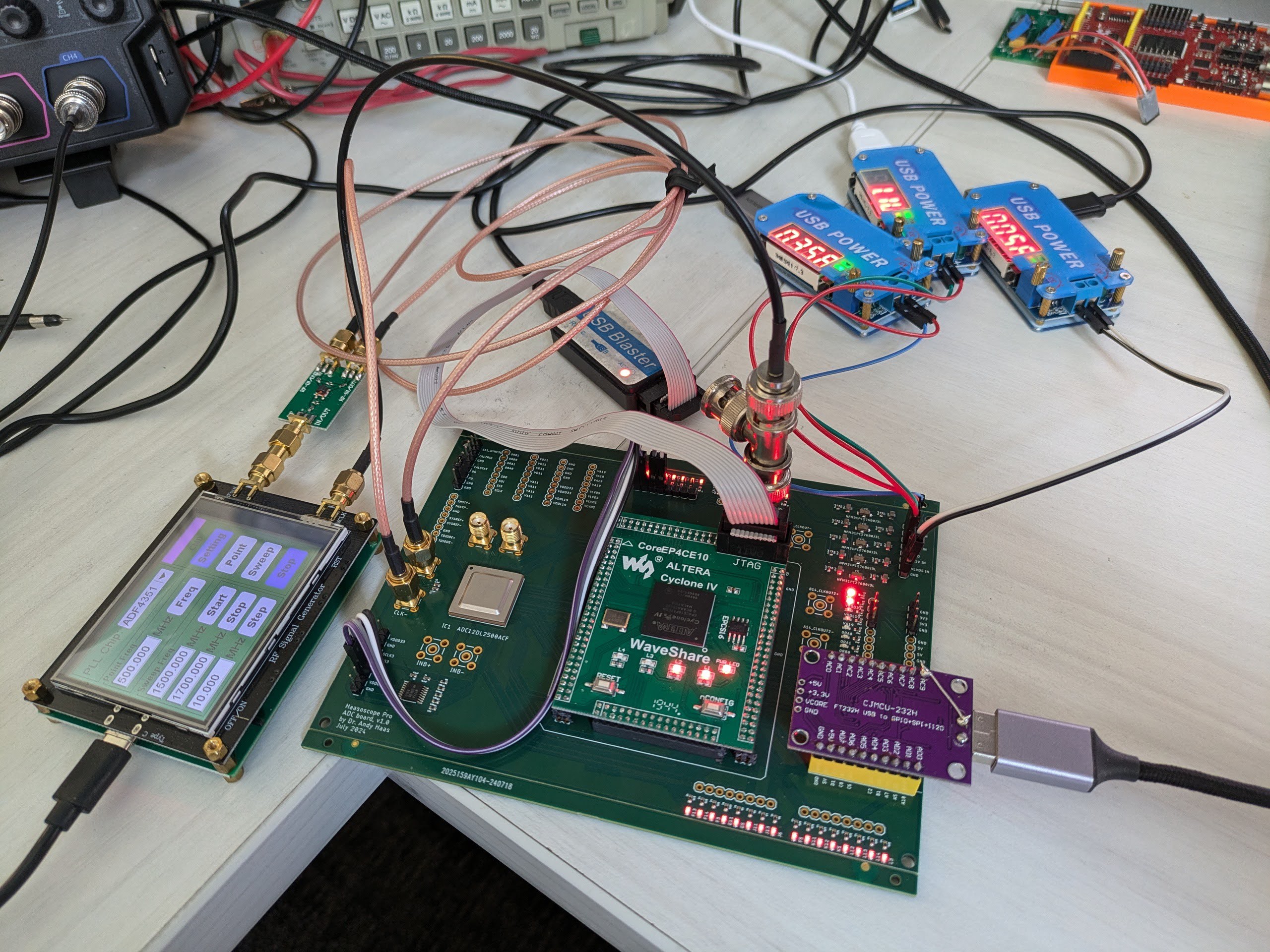
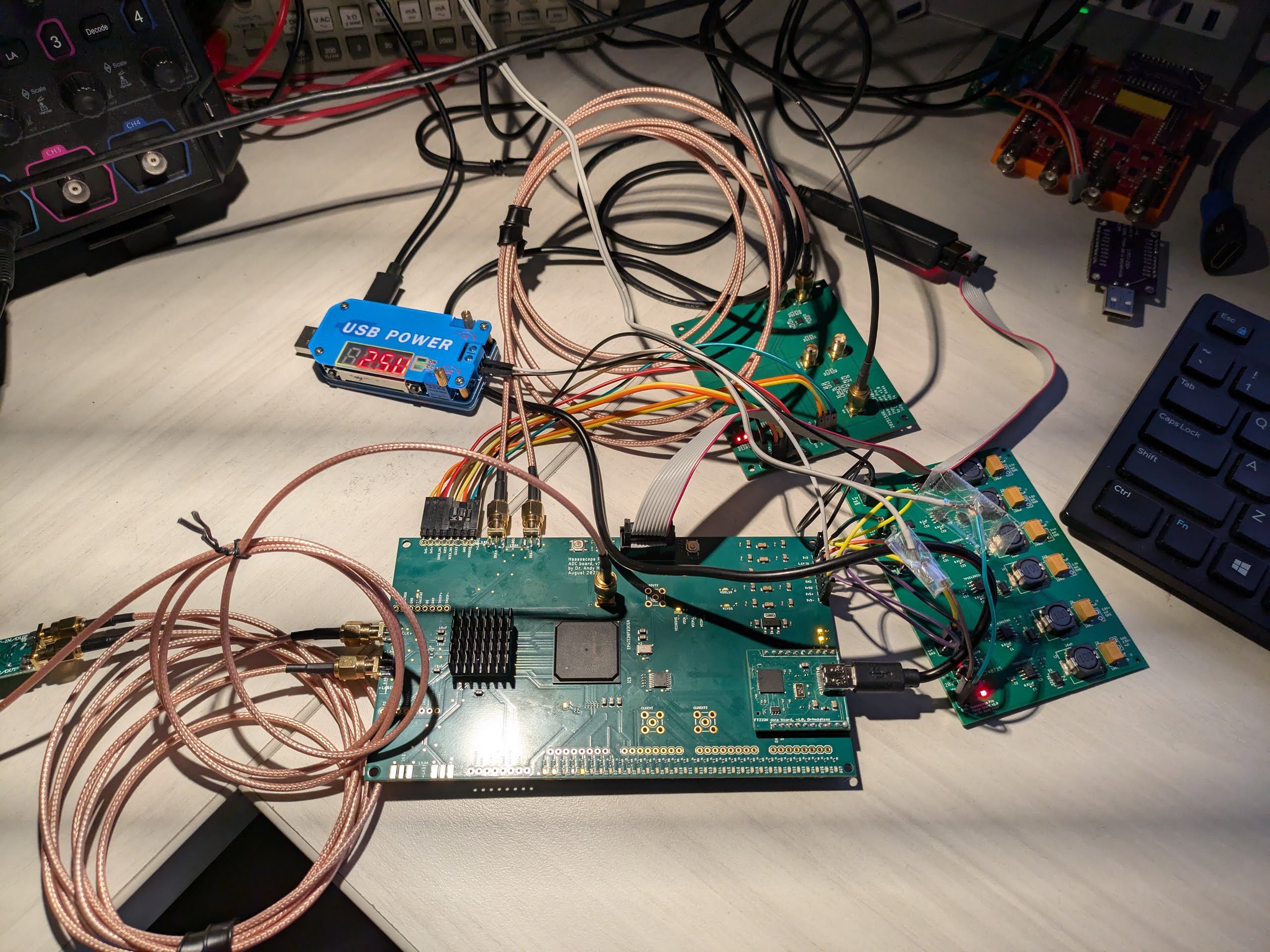
This is what the board looked like assembled, with everything attached to it. For power I was using these handy little USB-powered power supplies I found on Amazon to supply the ADC with 1.1V, 1.9V, and another 1.9V (separate for LVDS). The ADC also needs a very fast clock to tell it when to sample, 1.6 GHz. For this I used a cheap ADF4350 board from Amazon. But annoyingly it only had single-ended SMA output, whereas the ADC needed a differential output to two SMAs, so I used a cheap eBay single ended to differential converter. I also used another of these (not shown in pic) to input signals to the differential analog inputs of the ADC from my single-ended signal generator. To sync the clock between the FPGA and the ADF4350 board, I output a 50 MHz clock from the FPGA (big BNC connector sticking up) and connected it over to the reference clock input of the ADF4350 board.

A lot of things worked! I could talk to the ADC chip over SPI just fine, reading back it's Vendor ID and serial number, setting its registers, and power it up and down. It could also see the clock from the ADF4350, and I'd see data coming over the LVDS lines into the FPGA. Below you can see the binary LVDS data coming in, when I'm sending in a 10 MHz or so pulse to the ADC analog input - I do see the bits going from 0 to 1 in unison on most of the LVDS outputs! It didn't work fast, only up to about 200 MHz, because those LVDS lines were hideous - very different lengths, going through tons of vias and even 2mm pin headers and who knows what on the dev board, and even unterminated. But it was more than enough to encourage me to move forward with the project.

The next major step was clearly to put the ADC and the FPGA on the same board, and do the LVDS connections properly.
A very important lesson I'd learned, the hard way, was to break large projects into as many small blocks as possible. Especially for large hardware projects like this one, you don't want to put everything on one board at first. Start with each block on its own little board. Then it's quick, easy, and cheap to iterate versions of each little board you're working on, without redoing the other boards that already work fine.
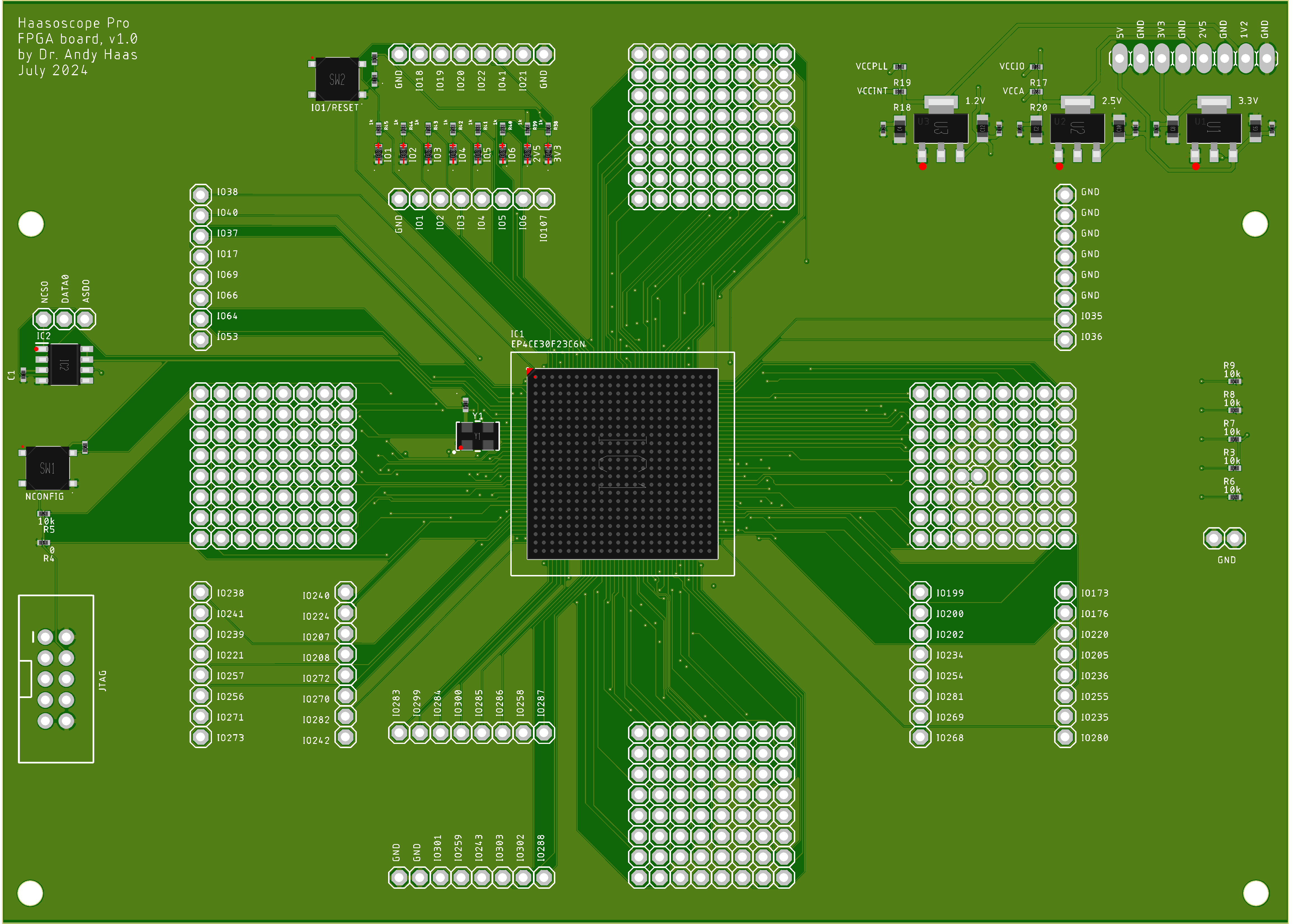
So I first made just a board with the FPGA on it, to get that working on its own. You can see a render of it below. It didn't really do anything except prove I could power it, program it with firmware over JTAG, see a 50 MHz clock input from the crystal, and make some LEDs blink. I also fanned out to .1" headers all the IO's, in case that would even be useful to me or others.
The board worked just fine, first try!

So then I was ready to make a board with an ADC and an FPGA on it, basically by merging together the first ADC board and the new FPGA board.
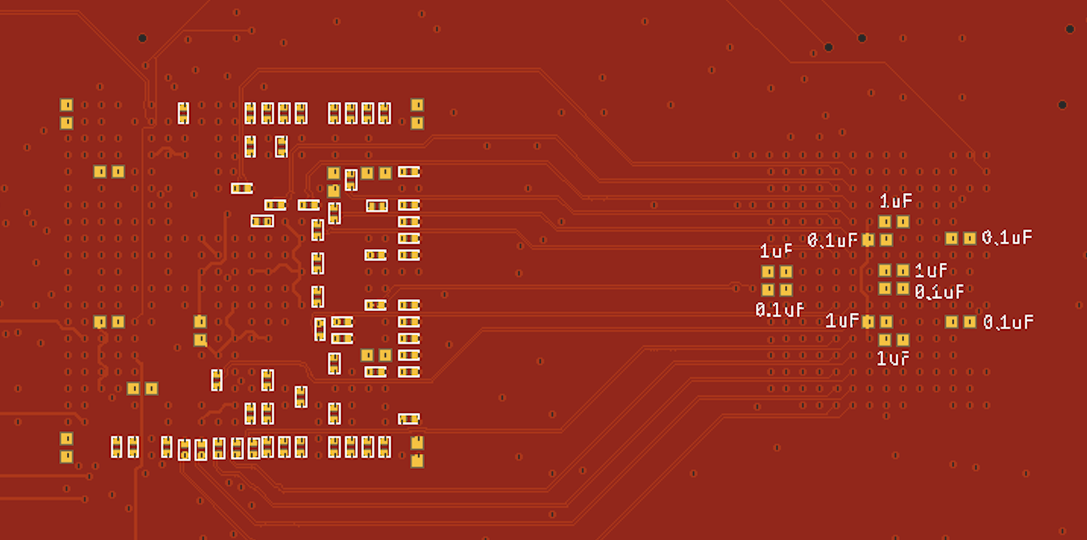
The LVDS signals from the ADC to the FPGA needed to have 100 Ohm termination resistors at the receiving FPGA side. That's 56 termination resistors, and they have to all be close to the FPGA. Some FPGAs have built in resistors for this purpose you can enable in firmware, called on-chip-termination (OCT). But the Cyclone IV chip I wanted to use didn't have that feature, nor the Cyclone 10, just the pricier Cyclone V. Fortunately, it turned out it was easy to add these resistors physically on the board. They just had to be 0201 size, and on the bottom of the board, directly under the FPGA, where each LVDS line came to two vias to get up into FPGA, as seen in the pic of the bottom of the board below. (The FPGA is on the left, and the ADC is on the right. You can also see the decoupling caps for both chips there.) But surely this would cost a lot extra, no? I'd now need two-sided assembly, top and bottom, and down to a 0201 package, not just 0402. Nope - JLCPCB gives free two-sided assembly and down to 0201 by default for all boards with 6+ layers!

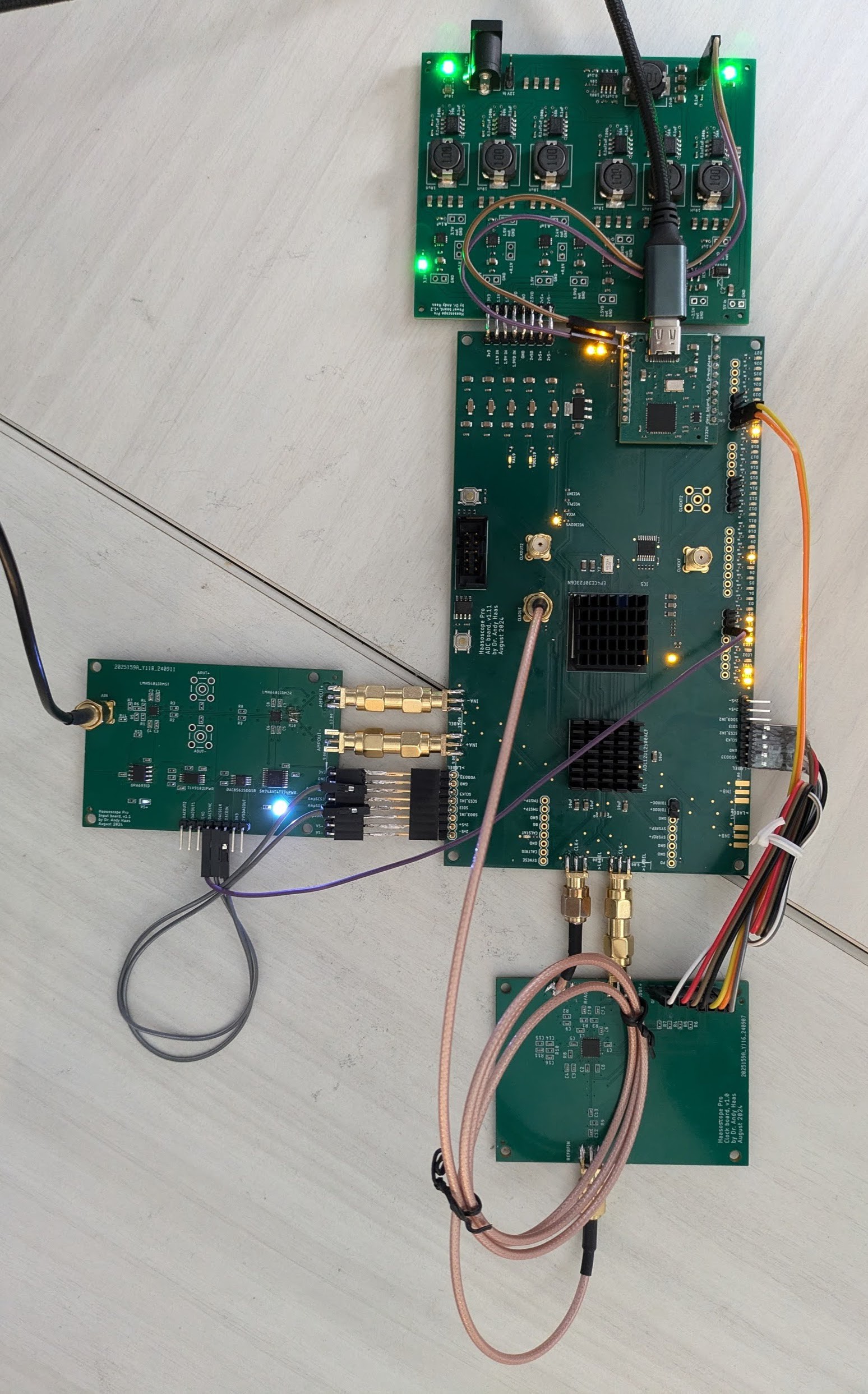
You can see below what the "ADC FPGA board" looked like in real life, with everything hooked up to it. There's now also a "power board" to provide the ADC and other things with all the voltages they need (on the right), an "input board" (on the top) to do the single-ended to differential conversion plus amplification of the analog inputs to the ADC, and a "data board" to replace the purple Amazon FT232H board that talks over USB2 to the FPGA. I still have one Amazon power supply for the FPGA since I forgot to make 2.5V on the power board initially. The clock is still supplied by the ADF4350 board the same as before.

Even more things were working well here, as you can see below. I may have shouted out some expletives and then cried a little when I finally saw a sine wave on the screen from the Haasoscope Pro for the first time. :)

Next piece to tackle was the "clock board", to replace the ADF4350 board from Amazon. That turned out to be simple - I just copied the reference ADF4350 design (basically the same as the Amazon board, but without the screen etc.) and put it on my own board. You can see it on the bottom in the pic below. Things are starting to look a bit more neat and tidy! I also added some DC offset circuitry to the input board using a dual 16-bit DAC.

The last board I worked on was the pre-input board, that handles annoying analog stuff... 50/1M switching, AC/DC switching, attenuation, etc. You can see a render of it below, with 3 relays and some carefully calculated 50 Ohm traces. It mostly worked fine too, though I had to mess around with different relays, connectors, and photo mosfets to maintain the 2 GHz of bandwidth. I even had to buy a cheap but wonderful NanoVNA V2 PLUS4 vector network analyzer to debug it all!
By the way, all these individual test boards are still available in the GitHub in the "sub boards" directory.
The last step was just to combine all the test boards together onto one board, and we had the first full prototype of the Haasoscope Pro!
-
How it began
11/22/2024 at 19:16 • 0 commentsThe original haasoscope was great, and still is, but as time has passed (6 years!) there were many ways I thought of to improve it.
As I advanced in the kinds of projects I worked on, including high speed data acquisition for experiments at CERN, and one of the world's fastest random number generators, I found myself needing a much faster scope. I managed to get one, because I'm spoiled and have a great research budget, but I was shocked at how expensive they are. Even a probe was $1000+, at the low end!
I started investigating why this stuff was so pricey. What I found was- The market for fast scopes is smaller, so companies need to charge more per unit in order to recoup their upfront R&D costs
- They charge more because they can! A lot of the high end scope market is made up of companies and institutions, for whom money at the $20-50k level is not an issue
I dreamed of one day making my own fast scope, to finally allow "ordinary people" to tinker with high speed electronics.
I was inspired earlier in 2024 by an open-source 2 GHz active scope probe on hackaday. I printed and assembled a few of my own, and they worked great, for under $100 each! The probe was already half the challenge (standard x10 passive probes are limited to under a few hundred MHz) - now I just needed a fast, affordable USB scope.I did some research and initially hit some roadblocks. Most fast ADCs sent data out on high-speed serial links (12.5 Gbps+), which would require a "high-end" FPGA. Those can easily be many hundreds if not thousands of dollars, plus licensing fees for the software and IP, not to mention having to deal with assembling a 0.4mm pitch 782 pin BGA! I was entering a world of pain.
But I then found a TI chip, strangely affordable, that also had a parallel LVDS interface. I could then use a "low end" FPGA - there are plenty of them with 100+ LVDS pairs for under $100, and free software and no licensing. I still had to deal with a 256 pin 0.8mm pitch BGA and a 484 pin 1mm pitch BGA, and routing ~80 LVDS pairs, each running at 800+ Mbps, but it finally sounded doable in principle.
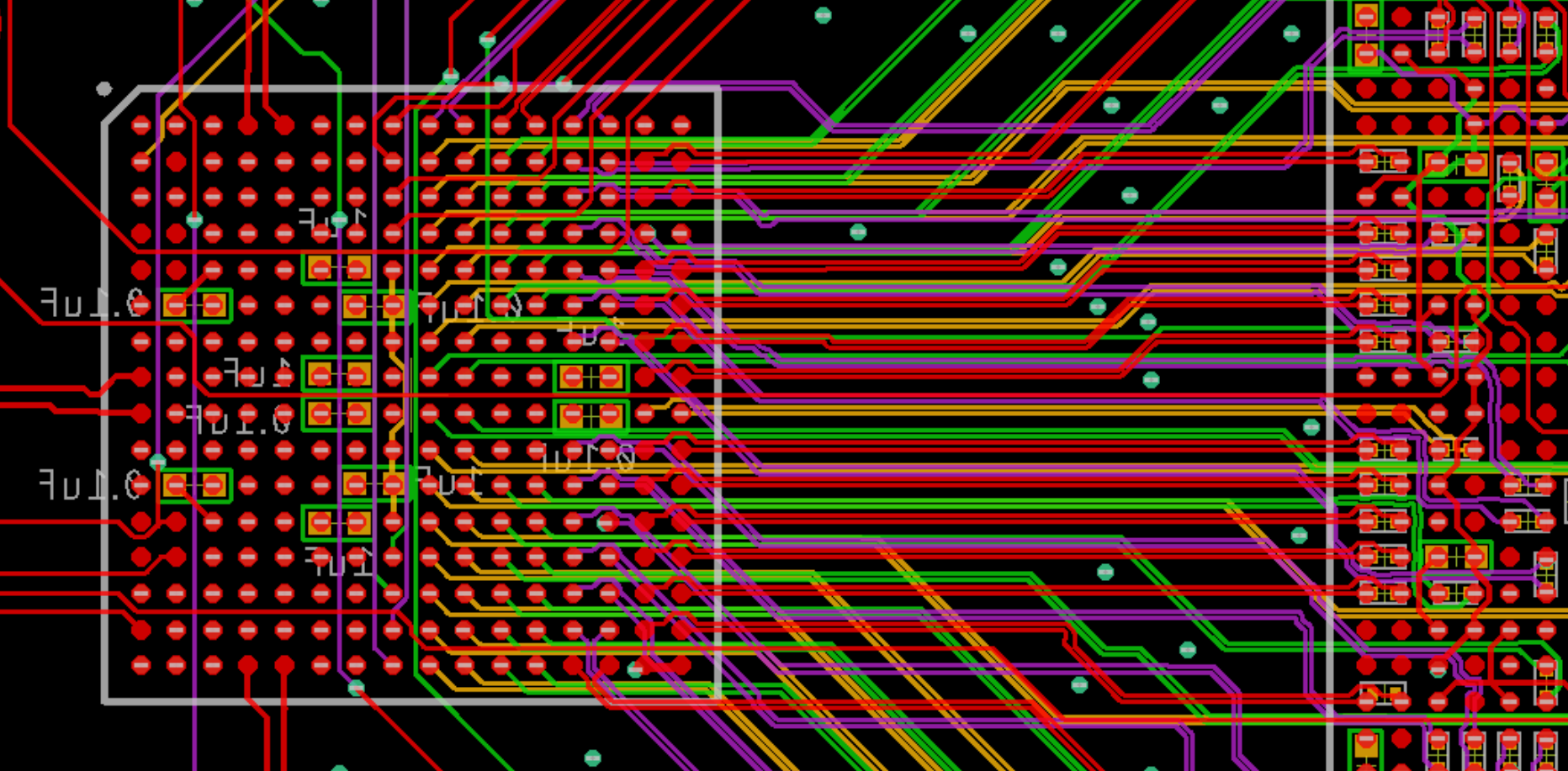
The routing was tough. At first I couldn't find a way to get all those signals out with less than 12 layers, and blind vias (as recommended in the data sheet / evaluation board layout). I priced it out and getting those made would be at least $500 /board in small quantities. (Blind vias are vias that connect only two specific layers of a multi-layer PCB, rather than holes going all the way through the board. They let you route other signals under (or over) the blind via, rather than having to go around it.) But I finally had a breakthrough and realized I could just get it to work, with only 10 layers, and no blind vias. I just needed thinner traces, 0.08mm (that's 80 microns wide!), and smaller vias, 0.2mm, directly under the BGA pads. Turns out that's just pushing the limits of some of the inexpensive Chinese PCB fabs, but they can do it! The boards can now be done for under $50 each in smallish quantities.

The last obstacle was dealing with those BGAs. The FPGA could be assembled overseas, but the ADC was not available in China. I priced out having a US assembler attach the BGA, and we were back close to $500 again. I wasn't going to pay that, especially for some prototypes, of which I'd likely need many iterations. Wait, could I assemble it myself?! I bought a reflow oven on Amazon for $300 and watched some YouTube videos. It didn't look that hard. After practicing with some cheaper chips, I finally tried attaching the ADC to my board. It worked! And the Haasoscope Pro was born.
 haas
haas