Bud Bennett
-
Working UPS-14500-IS Prototypes!
06/10/2017 at 22:07 • 0 commentsSome gremlin let the magic out of board #1. When I let the UPS charge the battery deep into the constant voltage phase the charger proceeded to overcharge the battery again. So the oscilloscope came out of storage and the hunt began. I'm seriously thinking that MSOP packages are not in my future. Here are the fixes that I made to both boards to get them working:
- I could not get the LTC4064 charging on board #2, so I replaced it with a recycled one from a previous revision. It still would not charge reliably (i.e. more than once). It turned out that some of the pins on one side were floating slightly above the board. When I checked them for connectivity the pressure from the probe caused them to sit on the pads and they looked good, but after the measurement they bounce back off the pad. I found the problem by rolling my fingernail over the tops of the pins and the charger started working. It seems like these MSOP parts either have too much or too little solder. Not great for hobbyists.
- The LTC4064 exhibited a bit of weirdness in the regulator loop. The PROG pin would occasionally jump from the normal 1.5V to about 2.2V and stick there -- this was what was causing the overcharging. (I think) it was fixed by increasing the bypass capacitor, C11, from 4.7µF to 10µF.
- Increased C7 to 47nF. The charger/booster race condition was still there when I checked the PWRGOOD signal with the scope. I had a 47Ω load on the UPS. If the wall wart was initially plugged in then everything worked and the battery was charged. If the wall wart was unplugged and replugged then the charger would not charge the battery. The scope trace showed a 2Vp-p sawtooth at PWRGOOD. The PIC did not care since it was set to have Schmidt-trigger input levels. But the charger has a shutdown threshold of around 1V and it was being toggled at a high rate. The 47nF allowed the PWRGOOD signal to ride through the transient produced by the booster.
- Changed R14 on board #1 to 0Ω and can now program the PIC in the circuit.
So now there are two working UPS-14500-IS units. I did connect one of them to the Raspberry Pi 2 (with a 16GB thumb drive and wifi adapter attached). It kept the power to Pi without any issues. I did not run any load tests and the Pi was essentially idling. The UPS held the power up for 1 hour 26 minutes! It also recharged the battery back to full in about 2 hours, as expected. I can't measure the safety timer but the timer's oscillator was still running 4 hours after it started charging, which is probably normal. The only problem I had was when I tried to use the push button to turn off the power to the Pi after issuing a "sudo poweroff" and unplugging the wall wart -- I had to keep the push button pressed for at least 5 seconds or the UPS would restart the Pi. I think that the wall wart has a large output capacitor that holds the input voltage to the UPS above 4V for a long time. The 5 second button press allows it to discharge enough that the UPS doesn't think that there is AC present.
I measured 42mV across the input switch when it was holding up a 1.25A load, so that puts the switch resistance at around 32mΩ.
The final tests are to see the size of the voltage droop when the wall wart loses power. I ran two cases:
![]()
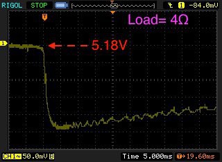
The above trace shows the output voltage droop when holding up a 4Ω load. The UPS output voltage, when powered by the wall wart, was 5.18V. The booster target voltage is set to 4.99V. The UPS allows the voltage to drop to about 4.94V before it catches it.
![]()
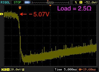
This trace is the same test with a 2.5Ω load (about 2Amps). The UPS output is now 5.07V, when powered by the wall wart. Some of that is due to the voltage drop across the input switch. The booster target is 4.99V. The UPS catches VOUT at 4.94V again. That's pretty good for a battery with nearly 0.4Ω of internal resistance.
At this point I'm satisfied with the performance of this board and calling it a wrap. It is doing everything I need it to do. I now need to code the routine that services the UPS in the background. Time to move on to the 18650 version, and possibly the "Hat".
-
UPS-14500-IS Early Results
06/08/2017 at 14:32 • 0 comments2017-06-07:
The latest PCBs arrived on Tuesday afternoon. I used the soldermask stencil this time and the TPS61236p went down easy, but the MSOP-10EP was still a mess of shorts. In fact I put too much heat on the part to try to remove the shorts and I think it is damaged. I ran into a few other issues as well. If I make another stencil I will reduce the openings slightly on the MSOP part (but I'm seriously thinking of not using the MSOP package ever again). Since I put solder paste over the entire PCB I had to work quickly to get everything attached. Some of the parts did not stick very well -- there were 2 resistors that were open and had to be resoldered by hand.
Some Issues:
First, I did not check to see if the correct program was loaded into the PIC -- it wasn't. The board did not work at all and for some reason I could not reprogram the PIC either. So I eventually desoldered the PIC and programmed it with the correct code, tested it on a breadboard, and then soldered it back on to the PCB. Then it worked.
The PWRGOOD indicator works well, as far as I've tested it, but I had to increase C7 to handle the no-load situation. I ran into an interesting race condition: With no load attached and the wall wart is unplugged, if the battery is charging then it provides a load until the PWRGOOD signal goes low and the charger is shutdown. With the lighter load the PWRGOOD signal pulses on/off (because C7 is too small to handle the pulse mode duty cycle of the TPS61236p) and that lets the battery charger cycle as well. I increased C7 to 10nF to stop this madness.
I've tested all of the functionality and so far it all looks good. No parametric data yet since I've just been using a 20Ω load.
This first board looked pretty good until I let it charge the battery to full. It overcharged it to 4.6V! I could not find the cause so I built another board -- this time I only used the soldermask stencil on the TPS and did the MSOP part by hand...still getting shorts. The second board won't charge the battery at all. At this point I think I'm going to try to replace the charger part with one of the LTC4064 parts that are on previous boards to see if that will work. I'm still hoping to get one of these boards fully functional. So close.I made the second board with shorting resistors for R9, R12 and R14 to see if that would correct the inability to program the PIC while in the circuit. It did, so now I'll have to go back in and replace those shorts one-at-a-time to see which resistor is preventing the program action. I suspect that it is R14 so that will get replaced last, if at all.
2017-06-08:
The charger on board #1 magically began to work today. I was able to charge the battery 3 times without incident. I'm thinking that the battery protection somehow misbehaved yesterday. With the charger working I could perform some discharge under load testing. The results are pretty much what I expected -- don't expect a small battery to handle a big load for very long. I'm using a KeepPower 14500 800mAh black battery. This is supposed to be from a reputable manufacturer -- I measured it's capacity at 722mAh when charged to 4.2V and discharged to 3.0V at 500mA. Here's the data:
Discharge test:Load 2.5 Ohm.
Initial 14500 bat voltage=4.00V
Battery dropped to 3.25V upon load (reported by I2C)
Initial Vout/no load = 4.99V
Initial Vout/w load = 4.94V
Duration = 2 minutes 54 seconds
Final Vout = 4.94V
Final Vbat = 3.0V (bounced back to 3.7V after shutdown)
Other observations: Booster IC and inductor were slightly warm to touch. Battery slightly warm. Reported battery voltage via I2C was stable and within 10mV of DVM.
Discharge test:Load 4 Ohm.
Initial 14500 bat voltage=3.99V
Battery dropped to 3.46V upon load (reported by I2C)
Initial Vout/no load = 4.99V
Initial Vout/w load = 4.95V
Duration = 13 minutes 22 seconds
Final Vout = 4.95V
Final Vbat = 3.0V (bounced back to 3.52V after shutdown)
Other observations: Booster IC and inductor were not warm to touch. PCB was slightly warm. Battery was warmer than electronics. Reported battery voltage via I2C was stable.
From the above data you can estimate the battery internal resistance at around 0.35Ω-0.4Ω. That's probably too high to support 2.5A. There might be 14500 batteries with lower resistance out there...
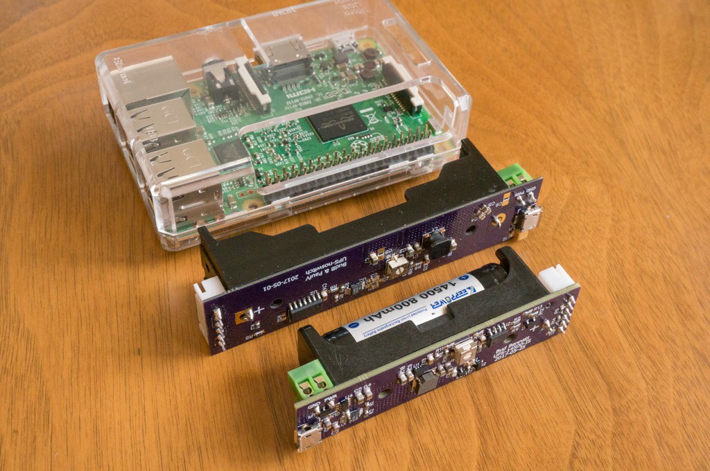
Here's a photo to prove that I actually built this thing. Compare the size with the previous 18650 version and a RPi3B. See how thin that inductor is? It costs 3x the taller inductor.![]() It's finally summer here. I have to do some Spring cleaning. The fish are calling...
It's finally summer here. I have to do some Spring cleaning. The fish are calling... -
TPS61236p Design Considerations
06/01/2017 at 21:01 • 0 commentsWhile I'm waiting for my PCBs to arrive, I thought it might be interesting to discuss the design considerations associated with the TPS61236p boost converter. This part is almost ideal for this application, though I wish that the INACT pin function was as described in the data sheet.
First of all...why the TPS61236p?...why not use the TPS61235p? Well, the TPS61235p has a fixed output voltage of 5.1VDC. This might work in a traditional UPS, but for this UPS concept having the ability to adjust the target output voltage is a big advantage. But the main attraction of the TPS61236p is the external voltage divider and the feedforward capacitor to adjust the response time of the boost converter. TI provides an application note about how to construct a feedforward compensation loop in this link. This is all well and good, but it is just a starting point. The TPS6123Xp has an internal compensation loop. TI isn't telling much about what the loop parameters are so they think they know best. They have an application in mind (probably some customer that is buying many millions of these things) and the rest of us can fend for ourselves.
Part of my experience was designing automotive circuits. There was almost no way that a 1megΩ resistor was going to be used in that environment unless the assembled PCB was conformally coated to prevent dirt/dust/humidity or other junk from compromising the resistor value. I'm using 30kΩ as a feedback resistor...so TI's suggested 10pF feedforward cap is just a starting point.
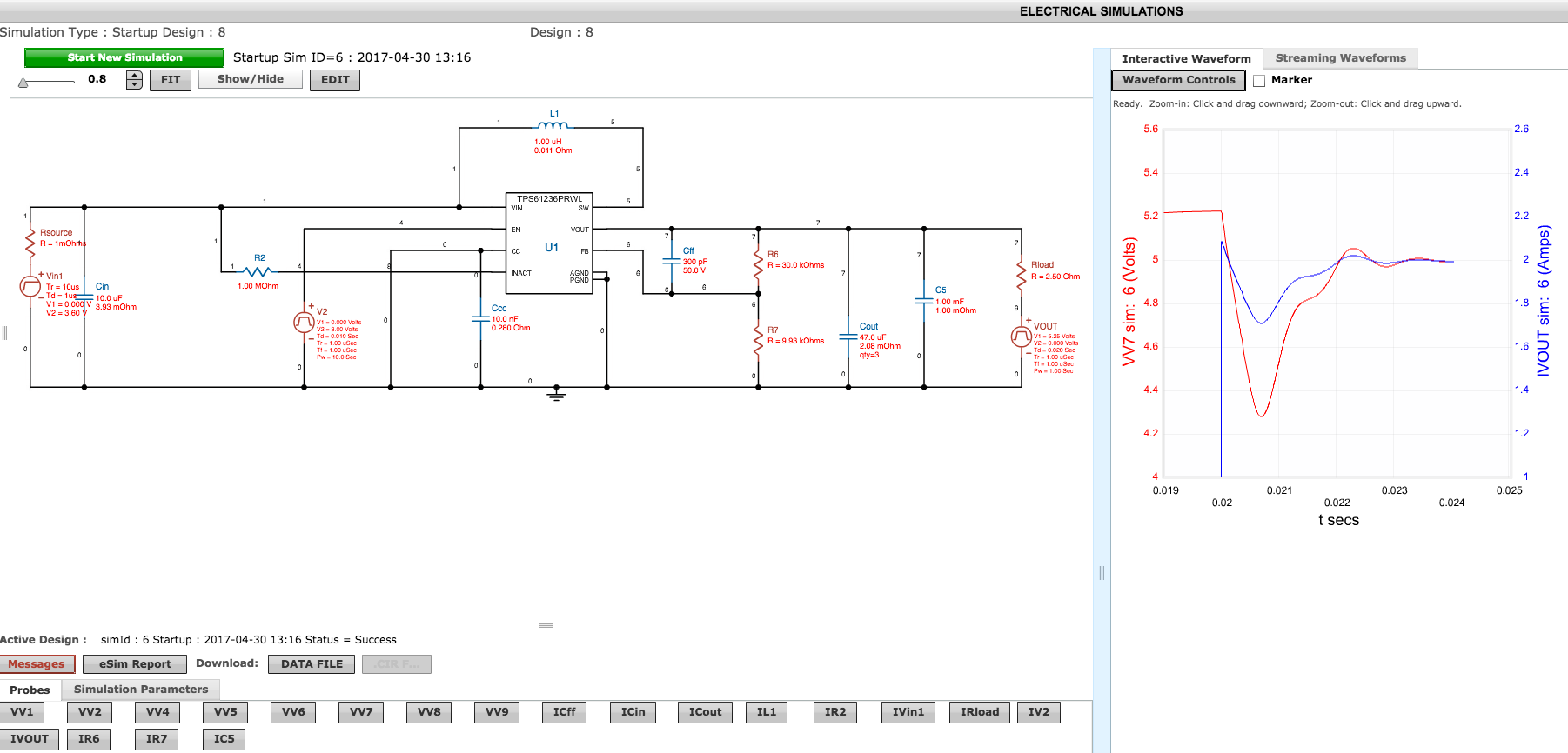
I discovered that TI offers a webpage that can simulate a TPS6123Xp application. If you click on the "simulate now" button at the lower right of the page it will transport you to their simulation environment. I found the simulation clunky and slow, but there was no other simulation option since TI did not make the TPS61236p model available for simulation on my desktop at home. I was able to setup my intended application and then adjust some of the component values to see what the impact was to the output voltage glitch (or droop) when the booster had to take over providing output power. I won't bore you with the entire process, but here's a couple of data points along the way:
![]()
The above screen shot shows my starting point. I was using a resistor divider 30x lower than what TI suggested, so I thought that a 300pF feedforward cap might be a good place to begin. The booster target voltage is 5.00V. The output load switches from being held at 5.25V, which keeps the booster off, to a 2A resistive load. Note the waveforms to the right -- the output droops to 4.3V, which would definitely reset the Raspberry Pi. And...the bit of oscillation afterward indicated that the system was barely stable.
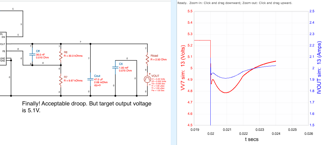
![]()
The above screen shot is near the end of the journey. I kept increasing the feedforward cap until I got acceptable droop -- in this case 200mV -- but I had to adjust the booster target voltage to 5.1V as a consequence. There is also a noticeable "long tail" response that is indicative of a right-half-plane zero. So I thought that I would insert a resistor in series with the feedforward capacitor to try to alleviate the RHP zero response. The result of that is shown below.
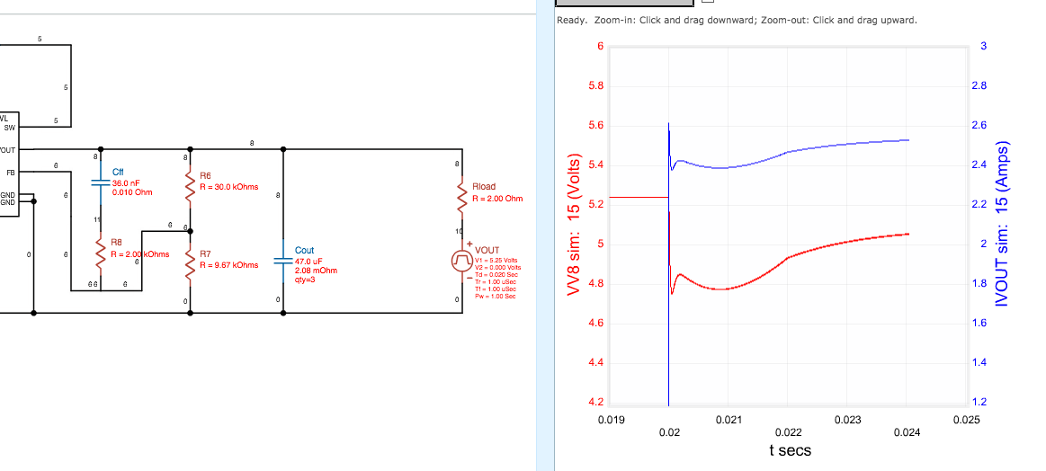
![]()
The effect of adding R8 in the simulation was not significant, but it wasn't a step backward either. I decided that this was "good enough" at this point and called it quits. I left the series resistor in the schematic as a CYA -- another variable to play with in case things did not go as planned.
The takeaway from this little bit of analysis is that without the feedforward capacitor, which is only available by using the TPS61236p chip, the output droop when the booster takes over providing power would probably reset the Raspberry Pi. Therefore, the only option was to use the TPS61236p and not the TPS61235p.
Since I don't have a 36nF ceramic capacitor in my inventory I specified a 33nF for the initial design. When I built the PCB I populated a zero Ω resistor in series with Cff (C13 on my schematic). After looking at the scope traces from the switchover events, this seems to be a good choice for the feedforward capacitor/resistor going forward.
-
Replacing the INACT pin function with something that should work.
05/31/2017 at 04:50 • 0 commentsI'm just figuring out how Hackaday projects should be organized. I will have to go back to the details section and clean it up to reflect the current project status. But this log will cover changes made to the first version of the UPS that uses the TPS61236p booster chip.
The INACT pin was supposed to be high if there was a light load on the booster, and go low when the booster a load current greater than 50mA. Unfortunately it didn't work that way. Here's my theory: the INACT pin function requires the booster to be switching in the low current burst mode. When the wall wart is providing power it holds the output voltage slightly above the target voltage of the booster which prevents the booster from switching. Therefore the INACT pin doesn't work and is set low by the TPS61236p, which is the wrong state and causes the battery charger to be shutdown and the PWRGOOD status bit is incorrect when sent via the I2C interface.
The fix is to provide a PWRGOOD signal by sensing the switching action of the booster. Instead of revising the UPS-NOSWITCH design I decided to put the changes into the alternative design using a 14500 battery. This board is named UPS-14500-IS because it is designed for the smaller Li-Ion 14500 form factor and includes an input switch to disconnect the load from the wall wart. The layout on this smaller PCB is more cramped and therefore more compromises were made so I figured if this smaller board worked then the larger 18650 form factor would be a walk in the park. The 14500 battery has a capacity of around 700mAh, so the UPS is not going to provide hours of operation. The primary task of the UPS is to hold up the power supply for a minute, or maybe up to 10minutes, and give the Raspberry Pi time to shutdown its systems and power down so that no damage is done when the power is removed.
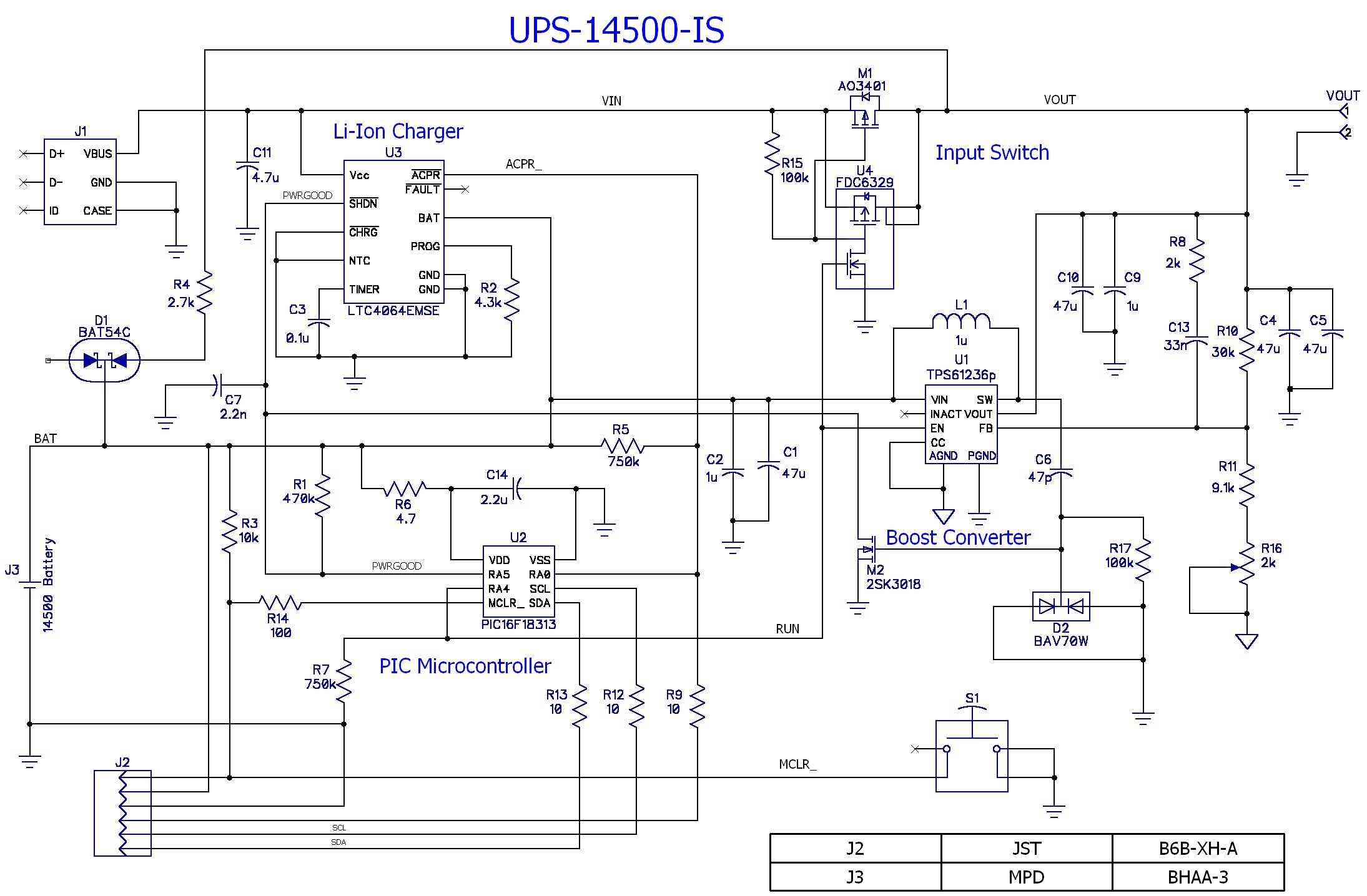
Here's the schematic of the UPS-14500-IS:
![]()
It's nearly identical to the 18650 design, but has the additional input switch circuit (U4, M1, R15) and the battery charger current is lowered to 350mA, which is the battery C/2, with a 3 hour safety timer (changes to R2 and C3). I will describe the other changes after covering the INACT pin fix.
Five components were added to fix the PWRGOOD signal function -- C6, R17, D2, M2 and C7. When the wall wart is providing power the booster is not switching and the SW pin is held at VBAT (the VIN pin potential). R17 keeps the gate of M2 at GND so it is in an off state and the PWRGOOD line is pulled high by R1, allowing the battery to be charged and the PIC to record PWRGOOD=1. When the wall wart power is removed the booster immediately begins to drive the SW pin, from 0 to 5V, at 1MHz. This action causes M2 to cycle on/off at the same rate and pulls the PWRGOOD line low after a couple of SW cycles. C7 filters out the switching frequencies and keeps the PWRGOOD line low -- even when the booster is in the low power burst mode. The purpose of D2 is to keep the gate of M2 from going too negative and keep M2 switching. D2 and M2 have to have low capacitance (2.5pF and 13pF respectively) so that the gate drive of M2 is not attenuated.
Other changes:
- Added R5 instead of using the internal weak pullup on the PIC input. This saves about 195µA.
- Changed R7 from 100k to 750k to save current. R7 is just to hold the PIC output low after reset to prevent strange behavior.
- Removed two input capacitors -- one not necessary and no room for the other. Only C1 and C2 remain on the booster input.
- Removed the 100uF output capacitor -- not necessary after testing the current UPS circuit.
- Added R4 and D1. This is a kluge circuit that injects current into the battery to compensate for the PIC current drain. The intent is to decrease the load on the battery when the wall wart is providing power and lengthen the interval between automatic battery recharges. It is more important to do this for this smaller capacity 14500 battery. This trick should increase the time between recharges by a factor of 2-5x (from 2 weeks to 1 - 2 months). Hopefully it will extend the life of the battery.
- Added the input switch. This 14500 battery won't hold up the power as long as the 18650. So there has to be some way to disconnect the power from the Raspberry Pi after it shuts itself off, otherwise the Pi could hang if the wall wart power came back on during its shutdown phase. Unfortunately the input switch causes a small voltage drop (and power loss) due to the 25-30mΩ switch resistance.
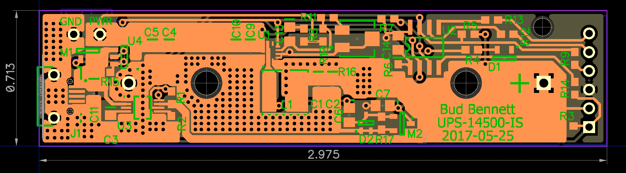
And here's the PCB layout that was sent to OSH Park to fab on 2017-05-26:
![]()
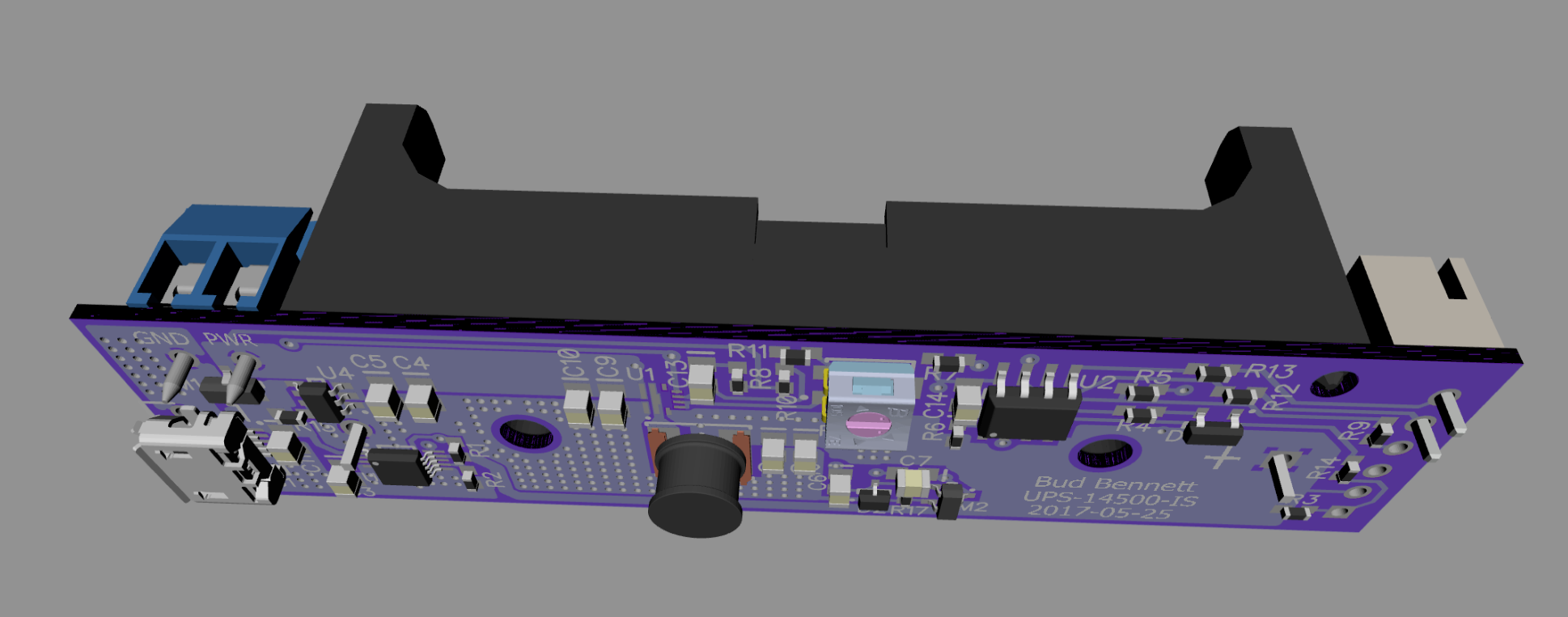
and the 3D view:
![]()
All of the circuitry fits under the battery holder. Top side components are the battery holder, output terminal block, I2C interface jack and the reset push button. This is a pretty small package -- less than 3/4"x3". The battery is equivalent to a AA battery in size. It is mounted by nylon stand-offs and screws/bolts in the two holes that go through the battery holder. I will probably use an inductor with only 2mm height instead of the 4mm inductor shown, as all of the other components are <= 2mm.
The PCBs should be back around 6/9. I'll publish the changes to the 18650 design in a subsequent log after I've finished testing this one.
Single-cell Li-Ion Powered UPS for Raspberry Pi
A simple yet complete UPS solution for most Raspberry Pi embedded applications, using a single-cell Li-Ion Battery.
 It's finally summer here. I have to do some Spring cleaning. The fish are calling...