Yann Guidon / YGDES
-
Adder with Falstad
03/05/2020 at 23:15 • 0 commentsSo Falstad is a reasonably potent logic simulator that lets me input schematics easily and test them.
I had hit a bug in the ALU8's CLA when porting the #VHDL library for gate-level verification back to #YGREC8 and went to other sides of the project, because I didn't feel the energy to go back through all the optimisations I made. But thanks to Falstad I can do it interactively...
So I went back to the main diagram and rebuilt the whole thing in Falstad's simulator:
![]()
The source code is so large I can't add it as a link so it's in the file Add8.cjs.
Slowly, little by little, I can resume the "bubble pushing" that created the nasty bug, but this time I can avoid it :-)
-
An unexpected but welcome tool
03/05/2020 at 11:37 • 0 commentsYou must know Falstad's circuitjs simulator, and I've been using it for some weeks for analogue designs. It's not perfect, I have found quite a few quirks, but this is also a logic simulator, not a highly powerful but capable and interactive one !
It took little time to draw the schematic of the INC8 unit and now I wonder why I wasted so much time doing it with Dia when I could also simulate the result and provide the source code (click here !)
![]()
With a few clicks I was even able to see where I made a mistake in the wiring.
I have stumbled upon a roadblock with the ALU8 and was feeling lazy to make a deep analysis of my mistakes, Falstad's circuitjs looks like the handy solution to that :-)
Now, is it possible to convert the netlist (extracted by my new tool) to display it with Falstad ? Or vice versa ?
-
Magnetic interferences
01/30/2020 at 20:35 • 2 commentsIt strikes me only now that I must have under-estimated the importance of magnetic interferences between relays...
I remember seeing placement recommendations for miniature Chinese relays but the РЭC-64 has a tubular shield. How do the openings at both ends behave ?
Having two relays on a well-spaced prototype breadboard can't show the effects of many relays packed densely and switching with weird patterns.
I'm starting to consider using mu-metal sheets but I wonder if it's practically effective and the right solution, because I still have some freedom to organise the parts in space and optimise the magnetic field...
Shoud I start playing with, or even build, a flux-meter ?
Update :
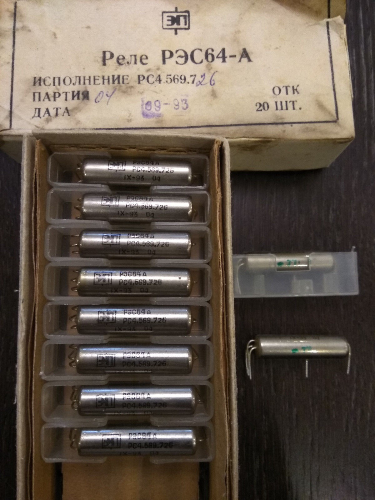
Here is the seller for the RES-64 :
https://www.ebay.com/itm/RELAY-RES-64A-726-REED-SWITCH-9-11V-NOS-USSR-LOT-OF-20PCS/232803573730
![]()
It's a SPST reed relay, you have the two contacts going out of the glass tube available at the opposite ends. The glass tube would be surrounded by the electromagnet coil, the whole is inserted in the metallic tube to further direct the magnetic field and shield a bit from outside influence. I still have to examine a non-working piece to confirm. An additional pin connects the "case" to ground (for example).
In the expected configuration, the relays will be paired and receive the same current, except during a set/reset pulse.
I'll have to check and measure the magnetic field at the ends of the relays. That's one excellent reason to finally use all those UGN3503 I bought for another project !
In the end, working in pairs might solve the problems I imagine so far.
One way to see it is with both relays forming a magnetic loop, to close the static field. I'll just have to find a way to loop the magnetic field, for example by cutting a torus in half. This ensures that the pair of relays is closely coupled, little energy will leak to the closest neighbours.
However, I suspect that the real problem is not the static field but the pulsed/forced changes when a capacitor discharges. This is what can affect sensitive neighbour relays but there is a catch : one relay is pulsed with the opposite polarity of the twin relay... In ALL cases, the magnetic pulse will go against the static field of one relay, while also reinforcing the field of the other relay. There must be an opposition of fields somewhere, a magnetic "hot spot" that can interfere with the nearby relays.
Ideally the programming pulse should have the same polarity for both relays. First it would prevent/limit the cases where one relay has a state different from its twin, in particular during power-on. Second : it would allow the magnetic pulse to be "looped" in a closed magnetic circuit, thus removing many causes of magnetic leakage and interference. The problem is that it would easily double the power drawn by the register set, since there would be 6V to be dropped in resistors... The whole register set would dissipate 2W instead of 1W.
Yes this log needs more drawings...
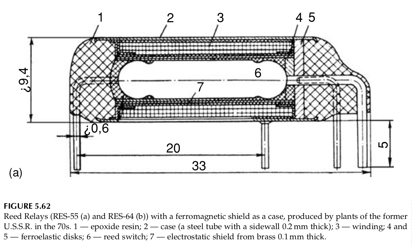
20200327 :I just found new information in a totally awesome book dedicated to relays !
![]()
The book is "Electric Relays Principles and Applications" by Vladimir Gurevich and it covers occidental as well as soviet relays. A truly fascinating encyclopedia that turns an apparently dumb device into a marvel of engineering !!!
Notice the element n°5 : what is a ferroelastic disk ? anyway it might prevent the magnetic field from escaping from one end, which is also great to reduce interferences from neighbouring switching relays...
-
And now, capacitors !
01/24/2020 at 16:53 • 0 commentsThe relay-based version of the YGREC-8 was in limbo due to delays in the delivery of required parts. I'm expecting more RES-64 to arrive in a few weeks, after ridiculous back-and-forth between post offices on strike. Meanwhile I was able to progress with #VHDL library for gate-level verification in amazing ways but... My soldering iron is asking for action !
Fortunately I received other parts from Russia (thank you eBay !) and I'm listing them to keep track of their intended use.
Those parts are pretty oversized, compared to today's technology, but the looks/appearance/style is worth it and the whole will be coherent ;-)
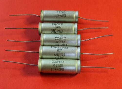
20× PETP K73-16 63V 2.2µF
These are non-polarised capacitors with medium value.
![]()
They are useful for 2 cases :
- for CCPBRL: the coupling between stages requires a capacitor but a polarised one forces the use of two shifted power supply domains. Non-polarised capacitors simplify the power supply design, as well as logic design in some corner cases. However, 2.2µF might not cut it for the RES-15...
- for the high-fanout buffers such as the ones described below:
![]() Some simulations with Falstad have shown that a high value would create an oscillation thatcould interfere with the rest of the circuit. A low value however wouldn't transfer enough energy from one side to the other. In both cases, the purpose is to prevent arcing at the contacts of the control relay at the bottom of the drawing.
Some simulations with Falstad have shown that a high value would create an oscillation thatcould interfere with the rest of the circuit. A low value however wouldn't transfer enough energy from one side to the other. In both cases, the purpose is to prevent arcing at the contacts of the control relay at the bottom of the drawing.
I don't think the YGREC8 needs 20 high-fanout signals but at least I'll be ready. The data memory system requires 5 buffers, the instruction memory might need a few more, but it is a reasonable approximation.
Of course I'll have to experiment, test, verify, measure... I expect to make another video when it's done :-)
Verdict : great surprise !
These capacitors aged very well and maintained excellent isolation as well as precise capacitance : +/- 2% worst case ! I don't know about the inductance but it should work very well.
20× Inductances Kig 0.1 1000μH
High-value, low-current inductors
![]()
These parts will "isolate" the various bitplanes from the main power supply.
Each of the 8 bitplanes contains at least 16 RES-64 to store the values from the register set, but these planes are quite sensitive to external interferences. A "pi" network is used : each bitplane has a local large-value capacitor, added to the large value of the power supply, and the bitplanes can emit and receive pulses that could flip other states...
The current rating is low but compatible with a single bitplane : each relay uses approx. 2.5ma, a total of 20mA, this gives a 5× margin with this 100mA part.
Verdict : good !
8.5-9.1 ohms is a bit much, but the inductance is around 960µH, a few percents of variation.
It should work well...
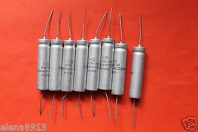
8x Capacitor K50-24 16 V 2200µF
high-value, medium-voltage power-storage capacitor
![]()
There are 8 of them, just as needed for the 8 bitplanes. Ideally they filter the power to the 16×RES-64. However due to the high capacity and the low current rating for the inductor, there is the risk of blowing up the inductor in the case where the input is (accidentally) shorted. A series germanium diode (or 2 in parallel for higher current capacity and longevity) would prevent the damage.
Verdict :
These parts aged but should be "good enough", with a self-resistance around 1M and average capacitance in the 1600-1800µF range. ESR might be high though. They can be for local power supply filtering..
Update:
I have "reformed" the capacitors through the slow and long application of current and the leakage has been significantly reduced.
I applied this method to the larger caps below as well.
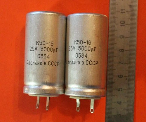
8× K50-16 25 V 5000µF
These big babies belong obviously in the power supply.
![]()
Not much more to say. It's going to be quite massive but I want to avoid as much ripple as possible.
There will be several voltages so at least a couple will be used for each rail, depending on the needed current.
Verdict :
something bad happened, probably a breach because there is liquid in the bag. Probably the electrolyte...
I'll have to get others and/or use my "modern" stock.
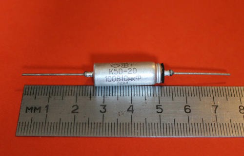
40× K50-20 100 V 10uF
Those are temporary bit storage caps for the Flip-Flops. 4.7µF would work too.
![]()
The value would be charged through a resistor (TBD) to reduce interference and spikes on the supply rail. The capacitor is discharged in the middle point of the two RES-64 in series, acting as inductors, so there is current reduction to add on that side.
Niobium is an alternative to tantalum, so the ESR is much lower than the electrolytic capacitors and it should be able "kick" the current pretty fast and counter the reverse EMF.
BTW : the + pole is at the black end (thanks @Artem Kashkanov !)
I need 8 of them for the write-back latch that feeds the write port of the register set, but other capacitors are required for the other Flip-Flops in the system, such as the PC counter, even counters, ...
Verdict:
Some parts seem to have a bit of gunk but appear functional.
Capacitance is good, ranging from 10 to 11.7µF.
Resistance/leakage is easily measurable (>1M) but good enough to work for short pulses.
Extra/leftover parts will reinforce the filtering of the power supplies.
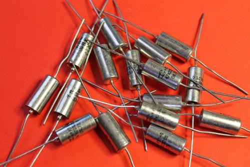
I also have received 30× axial tantalum K53-14 10µF 10V capacitors. The average capacitance is measured at 9µF (+/- 0.3µF) and it's smaller so more practical for the latches.
20× Niobium K53-4 20 V 47µF
Clearly useful to complement the large, high-ESR electrolytic capacitors for filtering the power supplies here and there (for the low and medium voltages up to around 12V). Two in series are mandated for filtering the 24V rail, made of a symmetric +12V/0V/-12V supply.
![]()
BTW : the + pole is at the black end (thanks @Artem Kashkanov !)
![]()
Verdict :
These parts aged and even if one is 60µF, many others are under 47µF, in the 37-43µF range.
There is some tiny current leakage but these should be good enough, though.
So that's it.
It's going to be a bold, large, bloated but exquisitely exotic board...
-
Core state machine(s)
01/12/2020 at 21:07 • 0 commentsUpdate 20200711 : superseded by log 106. FSM update
"Meanwhile..."I'm considering writing a quick&dirty&short behavioural simulation of the Y8 core to get a refreshed higher level view (as well as an alternate platform that simulates faster to try code out). I've already written one 2 years ago but it left a lot to be desired. Today's core has a more refined ISA and many details have evolved and matured. And I have a cool assembler I can throw at more challenges!
The core is still simple, anyway, with "most instructions executing in a single cycle", with 2 exceptions :
- Write to PC (except SET and CALL that can write directly to PC and bypass the slow ALU path)
- LDCL/LDCH that need one more cycle to read the instruction memory.
and then you realise you haven't thought about LDCx writing to PC, which makes things even more complex but who would do it ? (well, if 512 instructions of the 64K space allow it, there is 1 chance in 128 it gets executed so it's not negligible).
A proper FSM is clearly required. And soon, it appears that it's not going to be a nice and tidy FSM like you see in tutorials because I need 2 FSMs.
- One FSM handles the instructions and the special cases : stop/inst/LDCx/WritePC.
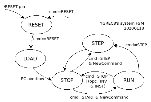
- Another FSM handles the execution state: start/step/stop/(re)set/load
These can't be completely joined because they are orthogonal. The execution FSM is what is visible from the outside, particularly during debug sessions. It must also handle internal initialisation when the chip goes out of /RESET (like: load data from external memory). The instruction cycle FSM cares for sequencing single and complex instructions.
So it makes sense to separate the 2 FSM because it untangles the complex combinations that might arise and prevents naughty bugs and race conditions.
Before going further, let's remind how the Y8 works : there is no real pipeline, yet 2 phases overlap:
- A first phase computes the next address (Increment PC) and/or gets a new address from an instruction, then fetches the instruction memory to read the next instruction.
- The second phase gets a ready instruction (or immediate word), then decodes/fetches operands/executes/writesback stuff.
The FSM must ensure that the instruction memory is fetched before starting the execution phase.
It gets more complex with the LDCx instructions because another round goes through the instruction memory. And if the destination is PC, yet another cycle is added to fetch the instruction instead of using PC+1.
OTOH, the core state FSM has to receive orders from outside, latch them and send the appropriate commands to the other FSM. Reset is asserted there, since no "general RESET" signal would be propagated through the whole chip, further simplifying the implementation.
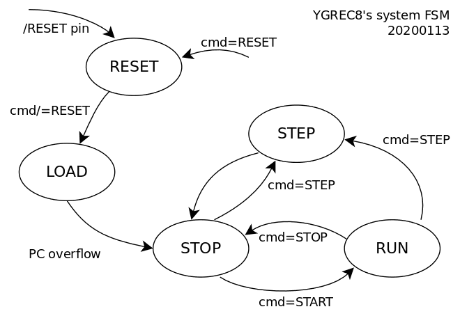
This FSM receives a code from outside and latches it before interpretation. During debug, it deals with the usual start/step/stop commands, though it defaults to start after power-up. A fourth command can be RESET to force a reload of the program memory (if you change the source code to debug or if INV wants to switch to a different code page).
So we get the following command codes :
Command code Description Start 11 Run the system Step 10 execute one instruction then pause the core. Stop 01 pause the core at the end of the instruction. Reset 00 pause the core and reset FSM
(reload instructions when another
command is received)The default command is Start when the core wakes up, and it can be modified (from input pins or through the debug interface).
The FSM can have more states to deal with initialisation. It is clocked by (and synchronised to) the core clock. Its value should be read back by the user after every command to ensure the proper value is latched and the FSM is in a coherent state.
The five steps (so far) are:
State Description How to get there Reset Just do nothing.
Clear PC and some
eventual SR flags.receive the RESET command
or external signal.Load copy external data to
instruction memory,
increment PC for each
new word.ext. Reset signal is
de-asserted and receive
command (other than Reset)Stop wait, do nothing. - Load is finished (PC overflow)
- received Stop when in Run
- when in state StepStep Execute one instruction - received Step command Run Let the core do its thing - received Start command
when in Stop state![]()
I hope it's clear.
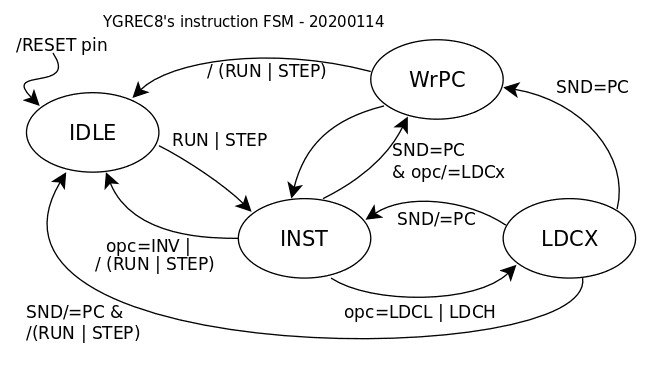
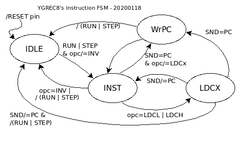
The instruction FSM has 4 states:
State Description how to get there IDLE Do nothing. - opcode=INV in state INST
- state/= Step and state /= RunINST decode and execute instruction - INST
- LDCX & SND /= PC
- WrPC
- IDLE & State=RUN or STEPLDCX cycle to read instruction memory state=INST and opcode=LDCH/LDCL WrPC extra cycle to fetch instruction state=INST or LDCX and SND=PC and opcode/=SET|CALL These states have different names to prevent confusion between both FSMs.
![]()
From there, the code is pretty easy to write...
Note : the split FSM makes them easier to run fast and less prone to bugs.
The size for storing the states is marginally larger, but the decoding logic probably smaller.
The significant difference is the latency and delay : there is about two clock cycles of delay between the arrival of a new command and the start of the execution of an instruction. This is not a severe problem because the debug interface will be significantly slower than the core.
Crude simulations shows the "Phase FSM" has a flaw that allows a transition from IDLE to INST when the opcode is INV. This condition should put the FSM into a different state that is exited when a new command is received... I'm updating the code & sketches.
![]()
![]()
This system will now clearly refuse to execute any INV instruction, even in debug mode.
-
New decoder for the ALU
01/02/2020 at 04:05 • 0 commentsThe ALU needs a new decoder because I changed the logic of the ROP2 unit... With a working decoder, I can re-implement the fault checker and validate all the opcodes.
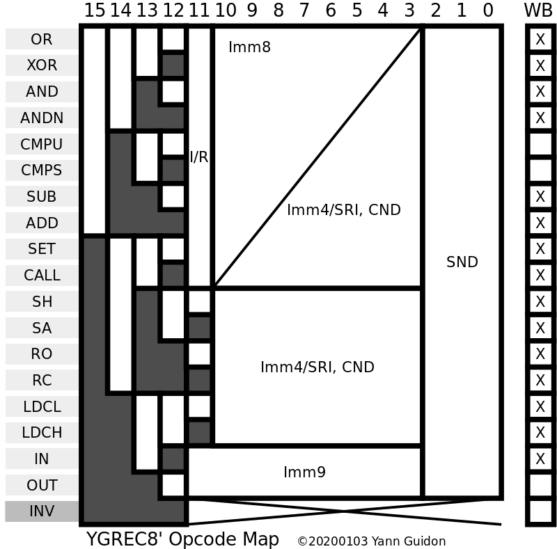
20200103 : I updated files here and there, as well as the main page that contains the "official definitions", because I have changed the order of the boolean opcodes.
![]()
I must make a new lookup table that is more thorough than the one at Bubble-pushing the ROP2 as well as the previous versions. There is a big difference, this time I use OR instead of MUX2 to combine the data so there are fewer degenerate cases.
       Func   NEG  PASS_en AND_en XOR_en OrXor_en  CLA_en CMPS  WB CryWr
OR     0000     0      0      0      0       1       0     x    1    0
XOR    0001     0      0      1      1       1       0     x    1    0
AND    0010     0      0      0      1       0       0     x    1    0
ANDN   0011     1      0      0      1       0       0     x    1    0
CMPU   0100     1      0      1      x       0       1     0    0    1
CMPS   0101     1      0      1      x       0       1     1    0    1
SUB    0110     1      0      1      x       0       1     0    1    1
ADD    0111     0      0      1      x       0       1     0    1    1
SET    1000     x      1      1      x       0 pass  0     x    1    0
CALL   1001     x      1      1      x       0 pass  0     x    1    0
SH/SA  1010     x      0      0      0       0 clear 0     x    1    0
RO/RC  1011     x      0      0      0       0 clear 0     x    1   b11 (RC)
LDCL/H 1100     x      1      1      x       0 pass  0     x    1    0
IN     1101     x      0      0      0       0 clear 0     x    1    0
OUT    1110     x      0      0      0       0 clear 0     x    0    0
INV    1111     x      0      0      0       0 clear 0     x    0    0
Some equations :
CLA_en = F2 & /F3
ROP2 = /F3 & /F2
F0F1 = F0 | F1
/F1F0 = /F1 & F0
/F1F3 = F3 & /F1
CMPS = CLA_en & /F1F0
CarryWrite = CLA_en | opcode=RC
RegisterWriteback = /F2 | /F1F3 | (/F3 & F1)
OrXor_en = NOR3( F1, F2, F3)
XOR_en = F0F1 & ROP2
NEG = ( ROP2 & F1 & F0) | (CLA_en & F1F0)
Cin = NEG (more or less but also need to decode ADD 0 cond)
PASS_en = /F1F3 & /(F2 & F0)
AND_en = PASS_en | (/F3 & /F1F0) | CLA_en
Maybe a 16×9 bits ROM would be better...
-
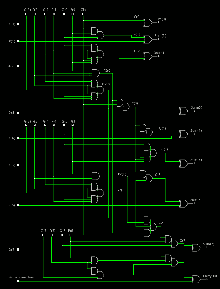
Pushing more bubbles, now the carry-lookahead adder
01/01/2020 at 17:48 • 0 commentsThe ROP2 re-engineering is going well, despite the surprising number of gates, but now it looks ready for an efficient ASIC implementation. So here comes the time for the ASIC-ification of the CLA...
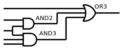
There is a 5-gates macroblock that appears 6 times in the circuit and it was already NANDified. See gate_CLA3.vhdl. As noted in the log Netlist and structure of the adder, we need to perform the function Y <= (A AND B AND C) OR (A AND D) OR E; several times and these need to be optimised as a whole. The following circuit:
![]()
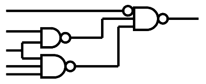
becomes:
![]()
but there is a remaining inverter...
Similarly, there are a few AND3 that would benefit from a switch to NOR3 if only the input was inverted.
And the AO1 gate ((A and B) or C) can also be turned into a pair of NAND2, if the C input is inverted...
Do you see where I'm going ?
So now, I'm adding a couple of new output ports to the ROP2 units that provide the negated version of P & G. The CLA circuit can then select the negated or positive version, which also decreases the fanout :-)
The ROP2 part has a pretty decent structure, despite the size.
Fanout:  Count:  .........|.........|.........|.........|.........|
    1 :     48 - ************************************************
    2 :     32 - ********************************
    3 :     24 - ************************
    4 :      0 -
    5 :      0 -
    6 :      0 -
    7 :      0 -
    8 :      5 - *****

 Depth:  Gates:  .........|.........|.........|.........|.........|
    0 :     21 - *********************
    1 :     16 - ****************
    2 :     16 - ****************
    3 :     16 - ****************
    4 :     16 - ****************
    5 :     16 - ****************
    6 :      8 - ********
It is quite easy to layout, with 2 gates "width" per bit.
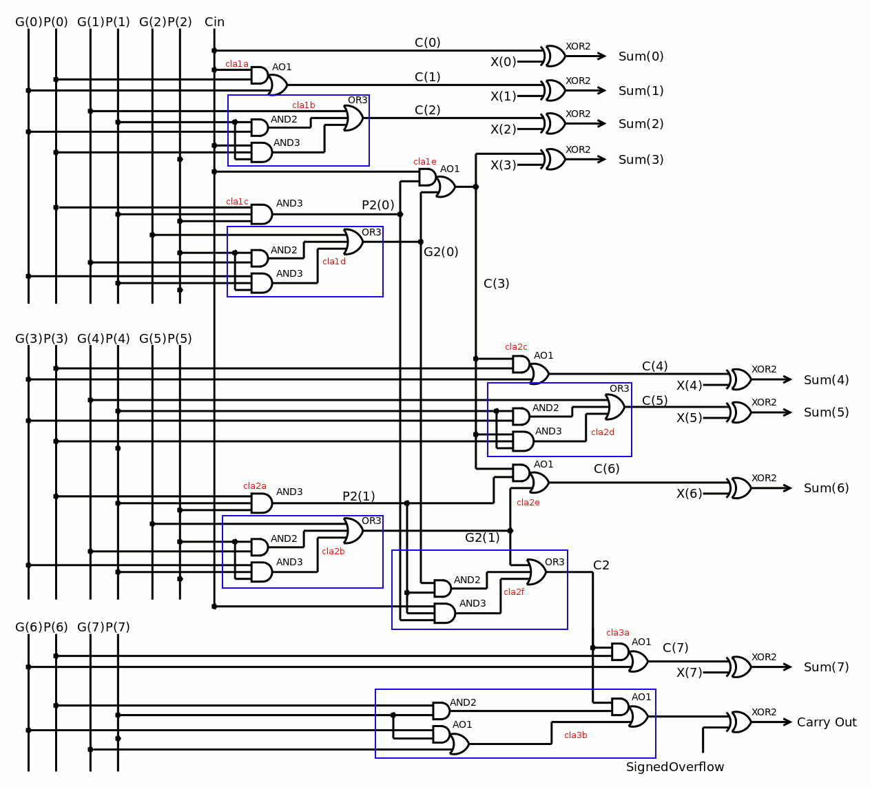
OTOH the carry lookahead is not as nicely regular and nicely behaved:
Latency of the 9 outputs :
    Output#0 : 2
    Output#1 : 3
    Output#2 : 4
    Output#3 : 5
    Output#4 : 6
    Output#5 : 7
    Output#6 : 5
    Output#7 : 7
    Output#8 : 8

************ END OF DEPTHLIST ************

Fanout:  Count:  .........|.........|.........|.........|.........|
    1 :     50 - **************************************************
    2 :     13 - *************
    3 :      5 - *****
    4 :      0 -
    5 :      1 - *

 Depth:  Gates:  .........|.........|.........|.........|.........|
    0 :     35 - ***********************************
    1 :     12 - ************
    2 :      5 - *****
    3 :      4 - ****
    4 :      5 - *****
    5 :      4 - ****
    6 :      3 - ***
    7 :      1 - *  <- the carry out
It is clearly not optimal but I wanted to keep the number of gates low. Only 35 this far :
![]()
Several places have their polarity (and gate type) swapped for an inverted version. For example: the signal G2(1) has been negated, so it drives cla2e and cla2f with their inverted input. cla2b is therefore totally swapped as well, made with NOR gates.
AO1 is usually replaced by AO1B so it can be implemented as a pair of NAND2.
The combined unit uses 123 gates !
Latency of the 17 outputs :
(the ROP2:)
    Output#0 : 7
    Output#1 : 7
    Output#2 : 7
    Output#3 : 7
    Output#4 : 7
    Output#5 : 7
    Output#6 : 7
    Output#7 : 7
(CLA8:)
    Output#8 : 6
    Output#9 : 6
    Output#10 : 7
    Output#11 : 8
    Output#12 : 9
    Output#13 : 10
    Output#14 : 7
    Output#15 : 10
    Output#16 : 11

Fanout:  Count:  .........|.........|.........|.........|.........|
    1 :     79 - **************************************************
    2 :     31 - ********************
    3 :     25 - ****************
    4 :      4 - ***
    5 :      2 - **
    6 :      0 -
    7 :      0 -
    8 :      5 - ****
 Depth:  Gates:  .........|.........|.........|.........|.........|
    0 :     23 - ***********************
    1 :     16 - ****************
    2 :     16 - ****************
    3 :     20 - ********************
    4 :     25 - *************************
    5 :     22 - **********************
    6 :     12 - ************
    7 :      4 - ****
    8 :      4 - ****
    9 :      3 - ***
   10 :      1 - *
The circuit uses these gates :
and2a ao1 ao1b inv nand2 nand3 nor2 nor3 or2 xor2
There seems to be room for 2 stages of OR between ROP2 and CLA8 output, to multiplex other values (from IN port and SHA/ROT)
Now I want to replace the output MUX and merge it with the XOR at the end of the CLA....
-
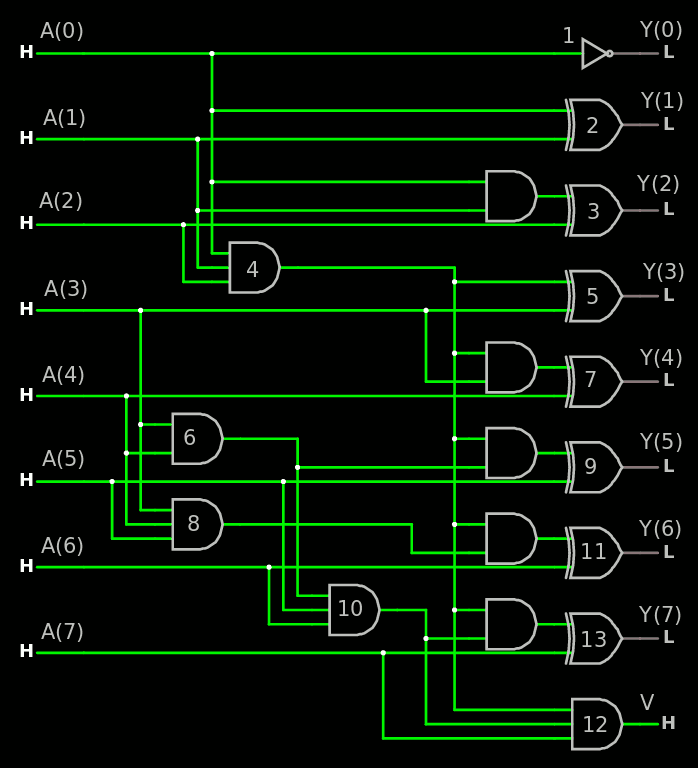
Bubble-pushing the ROP2
12/28/2019 at 22:43 • 0 commentsThe experiments with the RES64 are on hold, waiting for the delivery of more/new parts (and the strikes in France make the delivery date even more uncertain) so I'm back to the ASIC side of the projet. There is significant progress with #VHDL library for gate-level verificationand some early results are "interesting" and require more analysis.
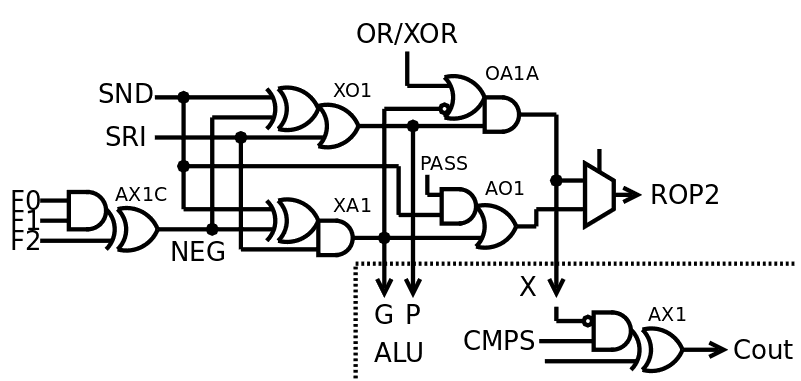
To ease this analysis, I'm forced to split the carry-lookahead adding tree from the ROP2/Pass logic, which I'm going to re-synthesise now. You might remember the log That ALU should be good (03/25/2019) and the following diagram :
![]()
Well, it works nicely with the A3P family's gates/tiles but it doesn't fly as well with full-custom gates. I tried to get the gates complexity down to simple ones (like NAND2 and NAND3), even trying to eliminate the output MUX2, and did some bubble-pushing.
Remember that this logic unit has deep ties with the adder logic : P and G provide the Propagate and Generate inputs, and the X output is used at the output stage as well. The rest is built around these fundamental, shared functions. I know well it is possible to create a boolean unit with only 4 NAND3 (see http://www.6502.org/users/dieter/a5/a5_2.htm) but that circuit provides only one of these functions at a time, when I need 3.
Another choice for the ROP2 part is to enable the output only when required. This makes ORing more practical, we can combine more data sources later with lower constraints (the fan-in is higher and the combining gates are less complex).
![]()
Starting from the output, I have made a big OR3 of AND2s, which were reduced to 2 layers of NANDs.
There are more control signals but this allows the output to be zero if nothing is enabled. More OR3s can be cascaded to inject data in the result bus.
I could push the bubbles further down the inputs but the P and G signals have a significant fanout so it makes more sense to simply put a buffer :
![]()
The other gates have a fanout of 1 (except the XOR2 at SND) so they can be simple, FO1 gates. The P and G gates can be OR and AND gates with FO4 or more, if needed, because they are a combination of a NAND2 and inverting buffer.
I have to redesign the control signals but that's not really a problem. There are more gates but they are "simpler". The new system is less adapted to ProASIC3 tiles but that's not the point. The new problem however is that when ADD/SUB is executed, the ROP2 output will contain the XOR value, which should be disabled somehow (if we want to use OR-combining only, not MUXes), unless another parallel NAND2 provides the value to the sink circuit...
The front-end XOR2 could be a XNOR2 if it's faster. In this case it's just a matter of adding an inverting buffer or something like that after the decoder...
OK, problem solved.
![]()
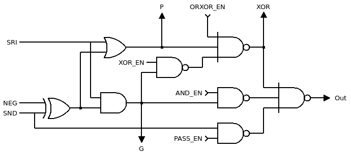
The XOR value is output unconditionally on the dedicated port, while the ROP2 output is cleanly enabled by ORXOR_EN, AND_EN and PASS_EN.
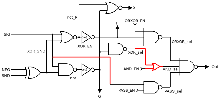
While implementing the unit, I found that there was some undesired redundancy :
![]()
The goal is to 1) reduce the fanout of G 2) avoid having 2 identical gates with one shared output, while there is "room" a bit later in the circuit.
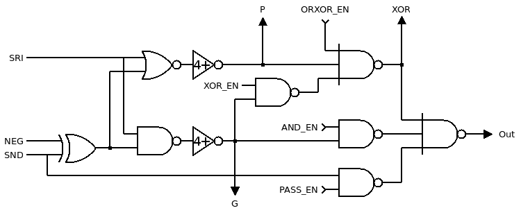
There would not be a MUX2, but probably a OR gate, which usually requires 2 levels of inverter but it's not in the critical datapth.
![]()
Decoding becomes a bit more complicated as well but... it will be easier for place&route :-)
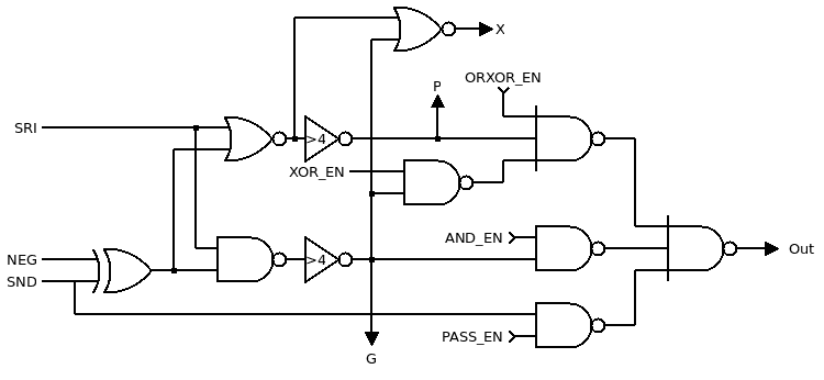
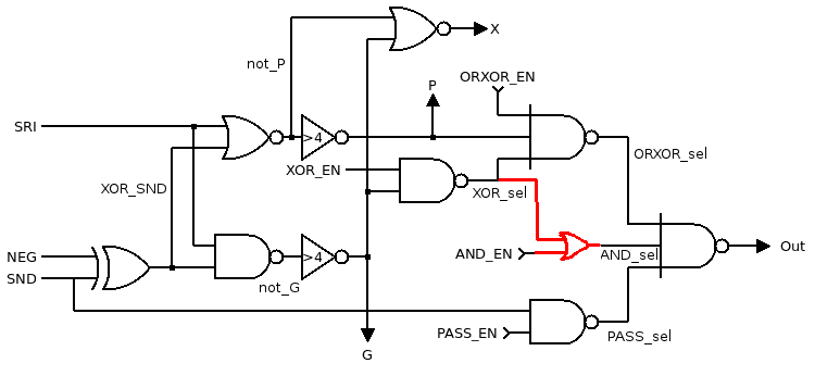
Erratum : SRI is the bypassed signal, not SND !
![]()
How did this mistake manage to survive this long ?
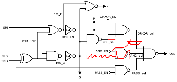
The truth table is pretty nice
       NEG  PASS_en AND_en XOR_en OrXor_en
OR      0      0      0      0       1
XOR     0      0      1      1       1
AND     0      0      0      1       0
ANDN    1      0      0      1       0
SUB     1      0      1      x       0
ADD     0      0      1      x       0
PASS    x      1      1      x       0
clear   x      0      0      0       0
Notice that I changed the order of the boolean operations (again) to make decoding easier.
I'll have to redesign the equations and decoder very soon.
ROP2 is 11 gates per bit, or a massive 88 gates for the whole unit. Fortunately it is quite easy to layout... -
A proper reset for the double-coil latch
11/09/2019 at 07:35 • 0 commentsA DPST relay can be emulated with two SPST relays, with their coils in series (one coil replaces the pull-up resistor so energy efficiency is increased). However there are two problems :
- the high-side relay gives an inverted value
- the power-up value of the complementary latch gives a non-complementary value, both relays are left open.
The first problem is somehow "easy" to solve with the YGREC8 : the inverted value will go to SND because there is a XOR/inverter in the datapath. We just need to invert "in the other case".
The 2nd problem is solved by a diode, connected to a common /RESET rail that is momentarily connected to 0V during the power-up sequence. This means more diodes, but the power-up sequence can be shorter than some code scanning the register set and writing to each of them...
I just tested my system with the RES64 and it works well. The only problem is the capacitance of the RS flip-flop, the 47µF capacitor I tried is too large and 5µF would be good (a discharge time of 10ms) though I can't find the appropriate part.
The discharge time will determine the max. switching frequency (?), I think 10µF would still take a full clock cycle to discharge at 50Hz, and nothing prevents us from aborting the discharge. So I ordered more Russian 10µF tantalum caps.
This is also interesting because the much higher resistance of the RES64 coils keeps us from having to use large capacitors for timing purposes. For example, the POR (Power-On-Reset) could be controlled by a large capacitor (1000µF ?) discharging in a coil...
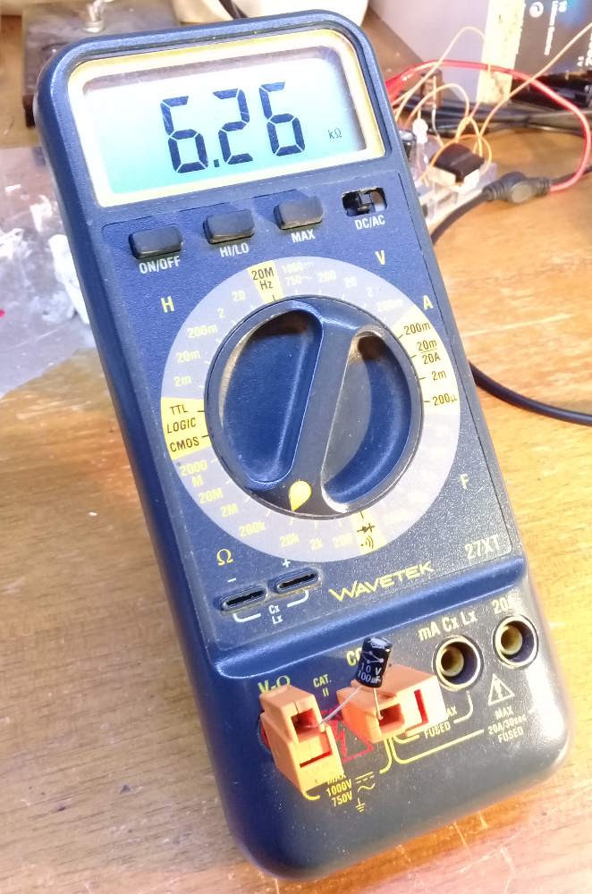
Experiments have shown very interesting results... Such as a 100µF capacitor with an internal 6K Ohms resistance ???
Because of this leakage current, the sensitive timing relay was still partially energised and wouldn't turn off after the RC time... Check your parts before using them !!!
![]()
No trick, I swear !
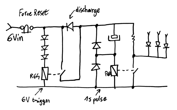
I make a 2-relays POR circuit now... Here is the schematic :
![]()
I botched the manual reset, is should be a SPDT switch so the 470µ capacitor is discharged fast (through 200 ohms or so).
The output has a weak pull-up resistor to backwards-bias all the diodes and (hopefully) reduce the crosstalk between all the latches.
3 more diodes help with discharging the capacitor or to prevent reverse-charging.
The 470µF cap provides a good 1s pulse.
The output RES64 could be buffered with more and stronger relays (like 3×RES15)
.........
The only problem is with the voltage trigger : this voltage changes with time and self-heat... I'll have to find another system.
Oh and the trigger voltage varies with the ramp-up speed...
But this system is still more reliable than nothing. And I can select how many Ge diodes are in series to tune the voltage.
Another challenge : how do I detect that the voltage has dropped below 5.5V ?
-
A new system for the register set
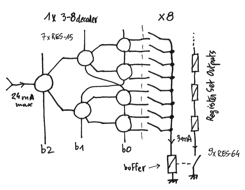
11/05/2019 at 21:24 • 0 commentsWith the new RES-64 reed relays, the intended circuit must be adapted. Then with the experience gained with the other circuits, I came up with a different system that has several significant advantages over the prototype I made 2 years ago... But there is one drawback : it takes MORE RES-64 and more room !
The write section doesn't change : each bitplane requires a MUX8 to steer the bit to the appropriate coil, plus the latching relay+capacitor, that's already 8×RES15 and 8×RES64.
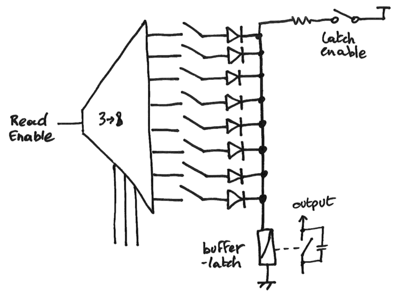
Reading however is different ! I simply took the large MUXes away, and I decode 3->8 with bipolar signals to select a whole register. I must add one diode per relay to prevent feedback loops but they are pretty small and cheap.
However there are 2 read ports and each latch must be duplicated because the RES64 are not DPST... that means a total of 144 RES64 !
Nothing crazy here, it's simply that I moved the MUX8 from the last to the first side, so it can be shared among the 8 bitplanes, which saves a significant number of relays.
![]()
Fewer relays make the system more dependable/reliable. The "sense buffer" (the same RES64 as the latches) needs less than 3mA and the MUX switches less than 3×8=24mA, the contacts are safe.
Of course it's not so simple : so many switches in parallel make feedback loops so we need diodes, one per switch, or 8 per bitplane, or 64 overall... But they are small and cheap so it's tolerable.
![]()
with the diodes, it might even be possible to use a bipolar system to save some decoding relays (MUX4 instead of MUX8), though it might be tricky...
It is also possible to latch the read bit, in case we need a pipeline latch or timing isolator.
But each RES64 is only a single switch and we need 2 of them, so unless I find a DPST reed relay that is similar enough, there are few choices :
- use/find/buy MORE RES64, which will take a lot of room
- use/find/buy more SIP reed relays (such as the Chinese ones I have found) because they are small and still cheap, though they break the "all-Russian style"...
- find a dual-switches reed relay... => unlikely.
This problem is specific to the register set because it has two read ports.
I/O and other registers have only one port (usually) so we can still use this method, for example for the scratchpad area.
Anyway, the huge parallel MUX8s were big annoyances and I'm glad I reduced their quantity. But I find myself with more questions to solve...
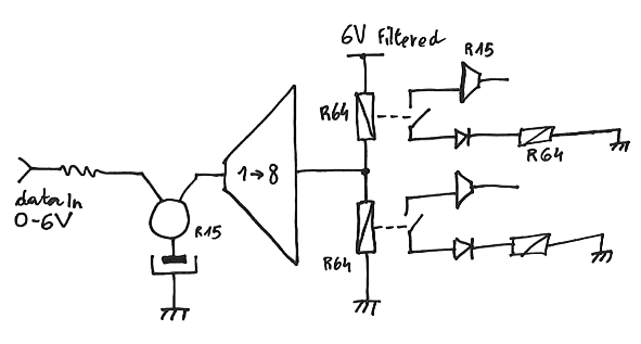
Lacking a proper, cheap, well-behaved DPST relay is not a catastrophe in itself. We can build one from two SPST relays by replacing the resistor with another coil, as in the sketch below:![]()
The system will be less "clacky" because reading one operand will switch far fewer contacts. Maybe it's for the best for our ears, but it's certainly better for the overall reliability : the fewer energised relays, the fewer power it draws, the fewer points of failure...
Furthermore : this diode-OR system could be useful to save a few relays here and there, because the SRI operand gets data from a MUX in the datapath. The "read enable" can be disabled if an immediate value (or anything else) is required by the instruction.
YGREC8
A byte-wide stripped-down version of the YGREC16 architecture