Yann Guidon / YGDES
-
A new assembler panel
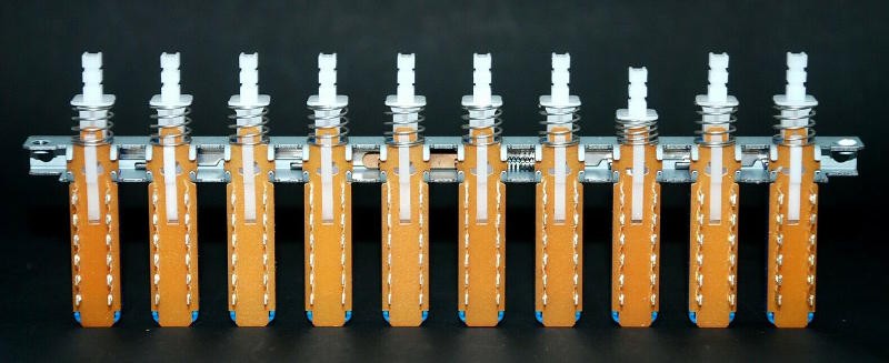
07/19/2019 at 23:11 • 0 commentsA few days ago, I had a blast from the past !
While looking for a multi-position switches in the local store, the clerk proposed a type of switch I had totally forgotten !
The impressive interlocked switch !
![]()
I initially wanted to use rotary buttons but you can't find all the options and it takes some turning...
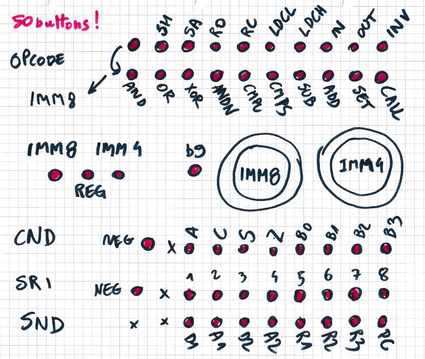
These buttons solve most of the problems I had, they use more room but they provide a direct access to everything. With about 50 buttons (and 2 rotary Hex encoders) one can select a whole instruction with a few pushes. Some rows or selectors can be enabled or inhibited, the conditions and the IMM knobs can be selected depending on the format selectors...
Here is the first sketch :
![]()
I just ordered more parts to start prototyping...
These switches are quite awesome. There are rotary switches but turning them all the time would quickly become ... hmmm...I keep the rotary selectors for the numbers but the opcode, the condition and register names now have their own button. These are not inherently linear things but symbols. So it's good to point directly at them and push the right button right away, instead of blindly turning a selector until it reaches the desired position.
The other advantage is more technical : these switches can come in 2PDT, 4PDT, 6PDT and even 8PDT ! This means that a lot of signals can be encoded directly at the mechanical level, reducing the amount of diodes and relays ! For the main parts I have chosen 4PDT and the IMM4/IMM8/REG selector is 8PDT.
-
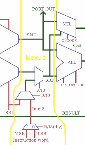
The nexus
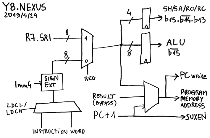
04/24/2019 at 18:37 • 0 commentsAs the register set and the ALU are (mostly) ready, now comes the time to connect them. This raises many questions that I hadn't considered fully until now and even though they are not really hard, they deserve to be treated carefully and independently from the rest. This is why I create a specific unit, which I name "nexus".
The primary purpose of the nexus is to gather all the operands and to fan them out to the sink units. So it's basic wiring, with the newly added twist to "control gate" the datapath ("data gate" ?). So it's wiring plus extra latches. And MUXes too...
![]()
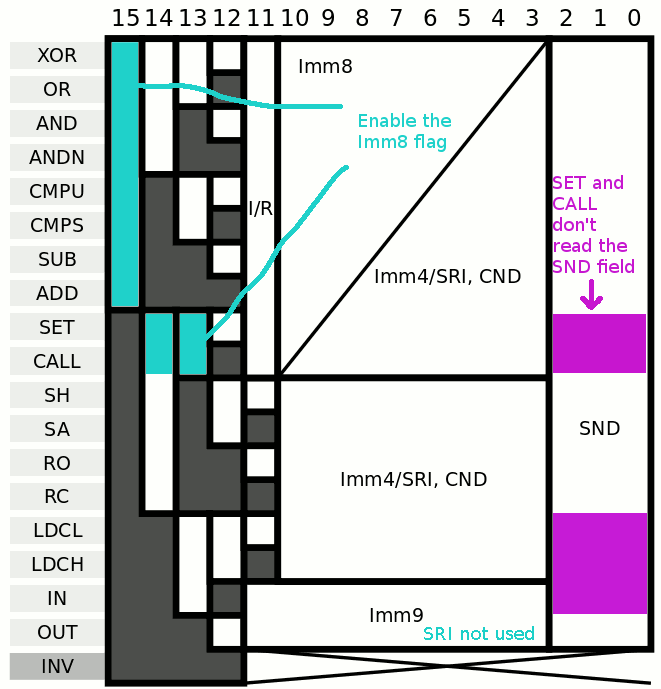
This is the part that mixes the immediate value from the instruction, with the SRI read port of the register set. With size selection and sign extension. And it must also handle the low/high part of the instruction word for LDCL/LDCH. Oh and it also must manage the crossover with PC (see the log Now faster without the "PC-swap" MUX)
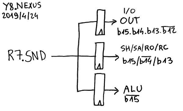
Let's first solve the easy case : SND is available directly from the register set and distributes it 8 bits to 3 ports, each with a latch:
- the I/O "OUT" port is transparent for b15.b14.b13./b12
- the "Shift" port (SH/SA/R0/RC) is enabled by b15./b14.b13
- the ALU port (CALL and SET don't use SND so it's simply decoded as /b15)
![]()
These latches isolate the buses and help solve fanout problems, on top of reducing spurious toggles in units where the result would be discarded. It looks great so far.
The SRI part is more complex... So let's look at a drawing:
![]()
The top half is the easy part:
- The register set provides the 8 bits on the SRI port
- SRI is latched to the shifter input, for the SH/SA/RO/RC instructions (b15./b14.b13)
- SRI is also latched at the input of ALU for 8 opcodes (/b15)
The other half is more sophisticated and subtle.
There is the part that writes to PC and sends the value to the program memory address bus. The PC is first incremented, then mixed with SRI for the SET and CALL opcodes so jumps and calls use only one cycle. But as explained earlier in Now faster without the "PC-swap" MUX, there is a 3rd case where the other opcodes write to PC but have a longer latency, the result bus goes to a bypass (btw, PC has its own write port).
Meanwhile, the incremented PC also goes to the result MUX (now called SUXEN, yes, it's a reverse NEXUS) because CALL must be able to write PC+1 to the result bus. This completes the crossover.
.
.
-
Census of the gates
04/21/2019 at 20:05 • 0 commentsIt's time for a little census.
[yg@Host-002 VHDL]$ grep -r 'entity' * |grep 'port' |grep 'map' |sed 's/.*entity //'|sed 's/ port.*//'|sort|uniq
AND2
AND2A
AND3
AND3A
AO1
AX1C
CLA3
INV
MX2
NAND2
NAND3
NAND3A
NOR2
NOR3
NOR3A
OA1A
OR3
XA1
XO1
XOR2
(I removed the complex unit names by hand)
There are 20 gates so far, more, and more complex, than what #Shared Silicon provides (only INV, NOR, NOR3, NAND2, NAND3 and some T-gates).
I believe that by using more complex gates with more inputs (but reasonably so), there is a bit of performance and size benefit. I don't see any roadblock to get the missing gates : either I can make mine easily, or I borrow from existing free libraries.
-
How to divide the register set's power consumption by about 5
04/21/2019 at 17:50 • 0 commentsThe latest source code archive contains the enhanced decoder for the register set, including 3 strategies:
- Straight (fast)
- update only meaningful control lines
- update only meaningful control lines when the related field is used
I provide a pseudo-randomised test to compare these strategies and the outcome is great:
[yg@Host-001 R7]$ ./test.sh
Testing R7:
  straight decoder:R7_tb_dec.vhdl:165:5:(report note): 100000 iterations, 702273 toggles
  latching decoder:R7_tb_dec.vhdl:165:5:(report note): 100000 iterations, 301068 toggles
  Instr-sensitive :R7_tb_dec.vhdl:165:5:(report note): 100000 iterations, 160231 toggles
R7: OK
There is a ratio of approx. 1/5 between the first and third result, which I explain below :
- Given that the probability of one bit being set is pretty close to 1/2, it makes sense that the first "straight" decoder toggles the output bits every other time in average. There are 14 control lines to drive and with a 1/2 probability, 7 lines change.
- The next method gives a better result, that you can understand using similar logic : we get 3 toggles per instruction, which makes total sense. There are 2 decoders but only 1/2 chance of change, so we can focus on one decoder. Each decoder updates only 3 of the 7 control lines because the other 4 give results that will not be used. So far, so good, no surprise at all.
- The last method gives an average toggle rate of 1.6 per instruction. This is one half of the previous result and though it should be taken with a lot of precaution, the benefit is clear. Some instructions (about 1/4) don't use the SND field, and the SRI field is not used when Imm8 or Imm4 fields are used, giving a further significant reduction of toggles.
Of course, these numbers are NOT representative of real use cases. I used pretty uncorrelated bits as sources, while real workloads have some sorts of patterns. The numbers will certainly increase or decrease, depending on each program.
There is a compromise for each situation and the 3 methods are provided in the source code, so you can choose the best trade-off between latency and consumption. The numbers are pretty good and I think I reached the point of diminishing return. Any "enhancement" will increase the logic complexity with insignificant gains...
-
A little note
04/20/2019 at 07:37 • 0 commentsI just thought about something else, which is a good argument FOR using a latch or flip-flop to drive certain control signals, in particular MUX2s:
MUX2 often needs complementary control signals. In A3P and other technologies, each MUX2 receives the control signal and implements an inverter inside the gate. However for ASICs can't always afford this luxury because the inverter would be uselessly duplicated, increasing latency and surface.
OTOH the latches and flip-flops usually work by looping two inverters back to each other and it's often possible to get the positive as well as the complementary output.
When signals are well routed, the control signal's latch can also serve as an inverter for free, there are 2× more signals (and double the load) but the logic complexity is reduced and uses fewer transistors. This is especially critical for the register set, to save room...
So while the FPGA version will use MUX2s for the latch and the register selector, the ASIC version will use a latch with 2 complementary outputs and the MUX2 is reduced to a simple gate that performs (A and B) or (C and D) (with for example B and D as control signals, using only 8 transistors in classic CMOS or 2/4 transistors with pass gates).
-
Control-gating the register set
04/19/2019 at 08:44 • 0 commentsThe logic strategy has evolved since 61. Making Y8 more energy-efficient with a deglitcher and the first code for the ALU is not yet satisfying, so instead of digging that part even more, let's shift our attention to the register set... A clean, fresh reboot of an old subject could work :-D
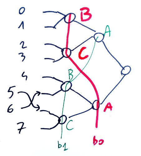
Let's start with a reminder about the structure of the registers: there are 8 bytes with 2 read ports and 1 write port and the write port shares the address with one read port (further saving instruction bits, but not control logic). For now we focus on the decode logic of the read ports, which we then duplicate to get the SND and SRI fields.
The register set is heterogeneous and uses multiplexers organised as a "balanced control balanced binary tree", seen in the picture below:
![]()
Address bits b0 and b1 are swapped at the middle of the tree to even/balance the load but control gating reduces this constraint (we still use this method because the fanout constraint is not eliminated). Bit #2 at the to of the tree is not affected.
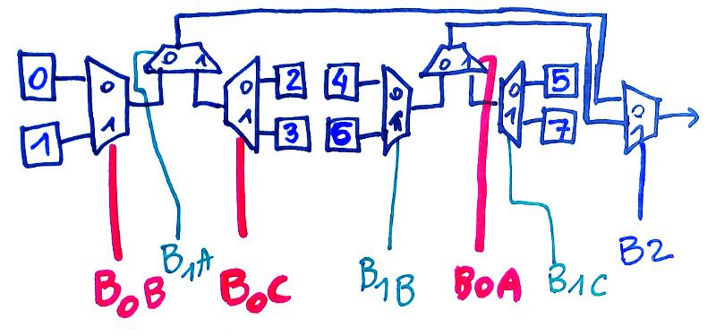
One bitslice uses two of these fancy "MUX8" to read the two operands:
![]()
Registers 5 and 6 are swapped, this is the only difference to remember. The address bits work almost like a normal MUX8, with the fanout slightly enhanced.
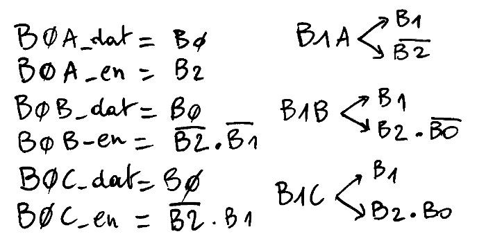
We are now interested by the enable logic : only 3 of the address bits need to be changed, out of 7, and only if needed. For example there is no reason to change B1B when B2=0.
![]()
So far, so good...
The register set is probably the most critical thing to decode As Soon As Possible so these simple equations are very convenient. But this is not the end of the story because another class of data can further inhibit the addresses:
- Some instructions (INV, IN, OUT) don't use the SRI field
- Other instructions (INV, IN) don't use the SND field
- The SRI field is not used in IMM8 or IMM4 form
The last one seems very easy to solve : bits #11 (R/Imm8 flag) and #10 (R/Imm4 flag) must be 0 to select SRI, so the Enable for the whole MUX8 must also AND with not ( Instruction(11) or Instruction(10) ). However this first approximation disables the 6 opcodes that don't use Imm8 (in particular the 3 opcodes that set bit 11: SA, RC, LDCH) and doesn't disable IN, OUT and INV (though only OUT sets bit 11).
However...
- IN, OUT and INV are not expected to be executed frequently enough to save significant power if control-gated. The few extra decoding gates do not a big deal but they add precious latency in the critical datapath.
- OTOH it is critical to correctly decode the instructions that don't use the Imm8 field. The bit #11 must be disabled when the opcode is after CALL or (conversely) enabled up to CALL. The last option is the easiest to code, with a 3-inputs gate : not(b15) or (not(b14) and not(b13))
SND is not used for the SET, CALL, LDCL, LDCH, IN and INV instructions. SET is likely the most used opcode so its gating might benefit the system. It is easily grouped with the neighbour CALL instruction with a 3-input gate (b15 & /b14 & /b13) :
![]()
LDCL, LDCH and IN can be easily added (b15 & b14 & /b13) and b14 is the only difference so the inhibition of reading SND is simply (b15 & /b13).
.
-
Scheduling (2)
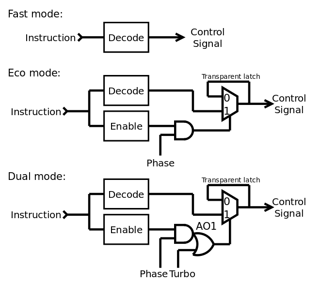
04/16/2019 at 06:20 • 0 commentsMore thinking and experimenting happened, as I faced a growing complexity with the decoding logic. There is the "fast" equation, then the "set" and "reset" ones, all must be written, checked, translated, mapped. And these equations are not compatible because there is no way to dynamically change from "turbo" to "eco" mode. The "eco" equations are too large and might still glitch a bit during decoding.
The conclusion is to simply drop the "set" and "reset" equations. I keep the "fast" equations and add a transparent latch ("T-latch") that gets selectively enabled by a new (single) equation (that indicates the "don't care"s). I see several advantages:
- Fewer equations to care about and optimise, fewer gates.
- 3 configurations are possible, where the "fast" equation is used all the time, while the "enable" gates can be discarded if only a "fast" version is implemented. A compromise is also possible, when the "enable" equation is forced to true in "turbo" mode.
- The "enable" equation can be a bit slower than the "fast" equations, which further reduces the chances of glitches.
- The T-latch adds little latency when data pass through.
- T-latches are quite easy to implement, using a multiplexer for example.
- You can get the VHDL code for the dual-mode version and let the synthesizer trim/prune the gates when you force/stick the "turbo" and/or "phase" signals to 1 (this is easier to configure, test, compare...).
![]()
It looks simpler and more flexible than the previous S/R scheme...
-
Scheduling
04/13/2019 at 21:24 • 0 commentsThe Y8 design works nicely with a standard, classic synchronous clock. It was indeed designed this way: each clock cycle would be a new instruction (with a few exceptions). This design is simple though a previous log (61. Making Y8 more energy-efficient with a deglitcher) shows that a more power-efficient (yet slower) method exists, using SR latches. Similar systems exist with transparent latches and the logical conclusion is to use a multi-phases clock.
In fact, a wide range of choices is available but I have barely scratched the surface, only looking for specific enhancements at specific places. For example I have only latched data at the instruction decoder level but other places would also be good targets : the output of the register set (with the IMM/REG MUX) and the result bus come to mind. Clock gating is nice but data gating is nice too :-)
A 4-phases clock (with many local gates) sounds like the best approach though it wouldn't account for the individual latencies of the individual stages. In fact, it is very similar to an unbalanced pipeline... This situation already appeared with the YASEP where a configurable pipeline was explored.
There are already several options for the decoder (either fast or latched) but I have to get ready for more options (and combinations). The clock generator's design will also follow from the chosen options. Fortunately the units themselves are not affected, only the connections between them.
In the current design iteration of the Y8, the instruction cycle is easily split into about 4 parts.
- The fetch/decode step : when the main clock goes up, the NPC value is latched by the memory block, the RAM is read and the value is fed to the decoding logic (approx 3 or 4 tiles). Given an access time of about 3ns and 1ns per tile, that first phase is around 7ns on baseline A3P.
- The operand read/select phase : lookup the register set and mix/select the immediate operand, going through approx. 5 tiles (or 5ns)
- The "execution" phase is at least 7 tiles deep, given the results of the ALU. Some headroom might be needed.
- The writeback evaluates the condition, checks the parity/sign/nullity of the result, MUXes the late units (and eventually latches the result). The result is fanout to the register set, which is subject to sample&hold constraints. That would be about 5 tiles long.
Using the worst case of 7ns per phase, the "minor clock" would be around 140MHz and the instruction cycle 35MHz. This could be bumped to about 45MHz if the writeback step overlaps the fetch/decode step. This is not very far from the estimated 49MHz of the unoptimised/unpipelined synthesis (13. First synthesis).
I'd like to offer at least the "simple/fast" and the "phased" options because one promotes speed while the other draws less current but most importantly is easier/smaller to implement in ASIC, since latches use less room that flip-flops (which are really just 2 transparent latches back to back).
T-latches are typically implemented by Actel with a MUX2 looped back to itself. ASICs prefer pass-gates, which is more or less the same. Sprinkling T-latches all over a chip is an old practice, because
- there is less load on the clock network
- 2 latches make a DFF
- T-latches use less surface and the register set would use 1/2 the surface than with DFF.
OTOH, DFF come for free with FPGA...
-
GHDL in a docker container
04/03/2019 at 12:12 • 0 commentsEthan Waldo has run the scripts successfully under Docker :-)
version: '3'
services:
  ghdl:
    image: ghdl/ghdl:ubuntu18-llvm-5.0
    volumes:
      - .:/src
    working_dir: /src
I have no experience with it but I'll add the above configuration file in the README.txt if people want to use containers.
GHDL has awesome strengths and it shows again :-) and it's only the beginning.
-
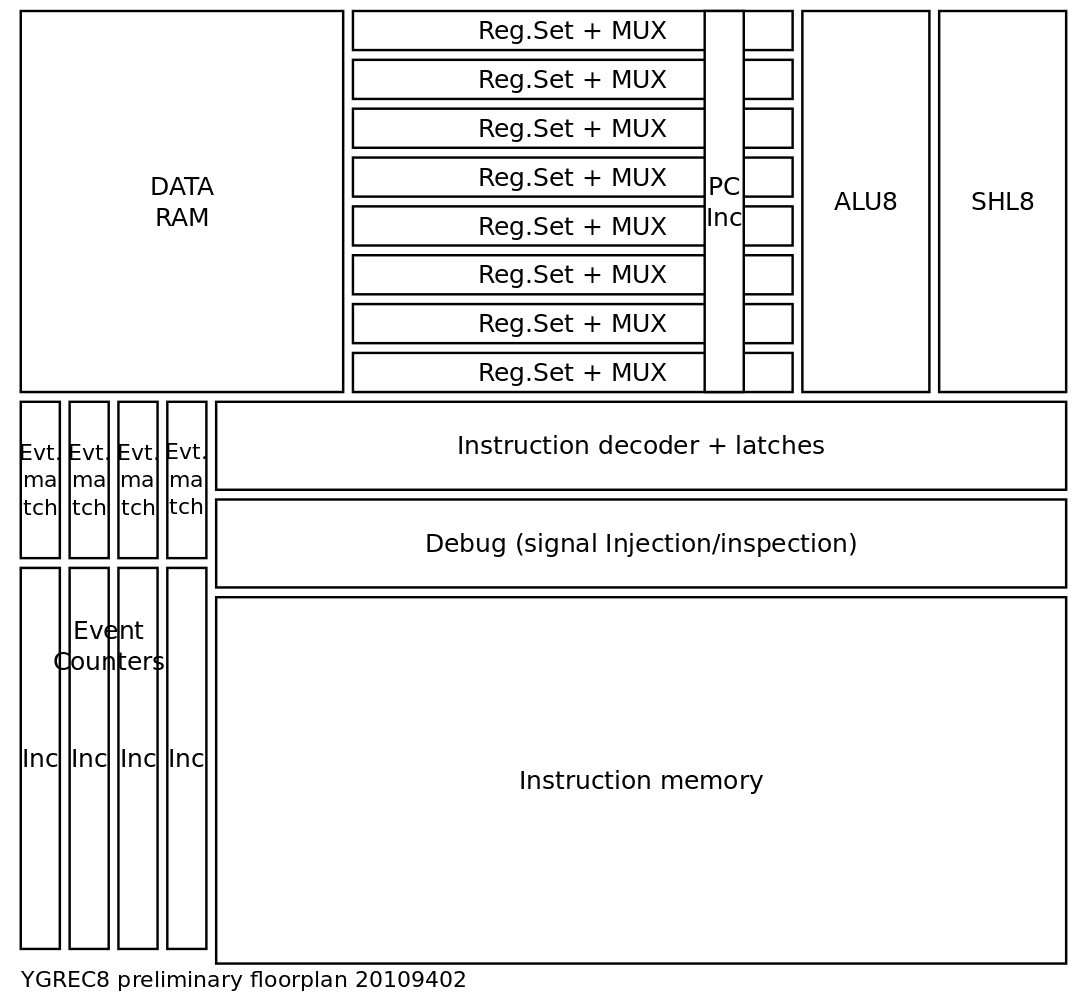
Floorplanning
04/02/2019 at 21:38 • 0 commentsSo far, here is the floorplan for april, targeting ASIC and FPGA :
![]()
FPGA doesn't need a floorplan (the synthesiser will try to "do something") but I want to try it, at least to 1) validate the intended ASIC 2) see if I can outsmart the synthesiser and reach higher speeds.
INC8 (increments PC) is done and ALU8 is mostly finished. I try to polish the instruction decoder. Once it's done, I'll easily bring SHL8 back from the older versions, and get a better latency estimate. This complete operating datapath is necessary to create the "final MUX" that creates the RESULT bus.
Not shown here is the I/O system. The address goes straight from the instruction decoder, using "partial address decoding", to the various units, and the eventual data to read is ORed/MUXed back to the datapath. This will take a lot of time/latency so this MUX comes last. There is no defined IO structure so it's hard to gauge...
.
.
YGREC8
A byte-wide stripped-down version of the YGREC16 architecture