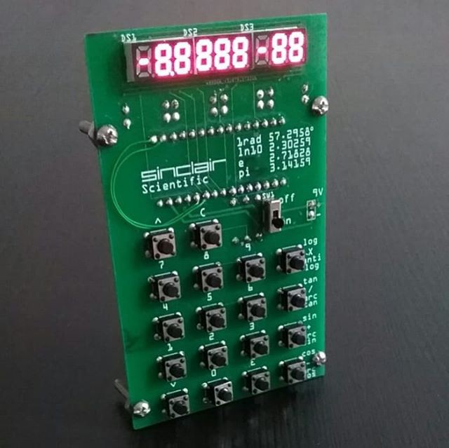
Arduino Enigma
-
01/17/2018 - Figuring out how to power this
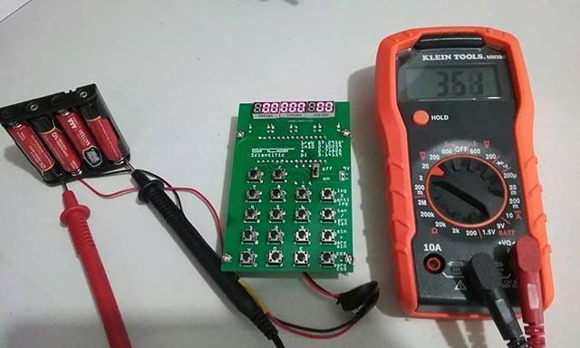
04/13/2018 at 04:43 • 1 commentInitially, a 9V connector was attached to the emulator. By attaching another 9V connector to different battery holders on hand, it was determined that as little as 3 AAA batteries would make it work. Since the original calculator uses 4 AAA batteries, and the holder fits underneath the calculator, I settled on 4 AAA batteries.
Next was an endurance test. The calculator was powered on and left to drain the batteries, 40 hours later, the drained batteries were measured to provide 3.54V. I am very pleased with this result. A new set of batteries will provide around 6V, for the Arduino power regulator to work all the way down to 3.54V is an excellent result. It begins to look like this will be a viable product.
![]()
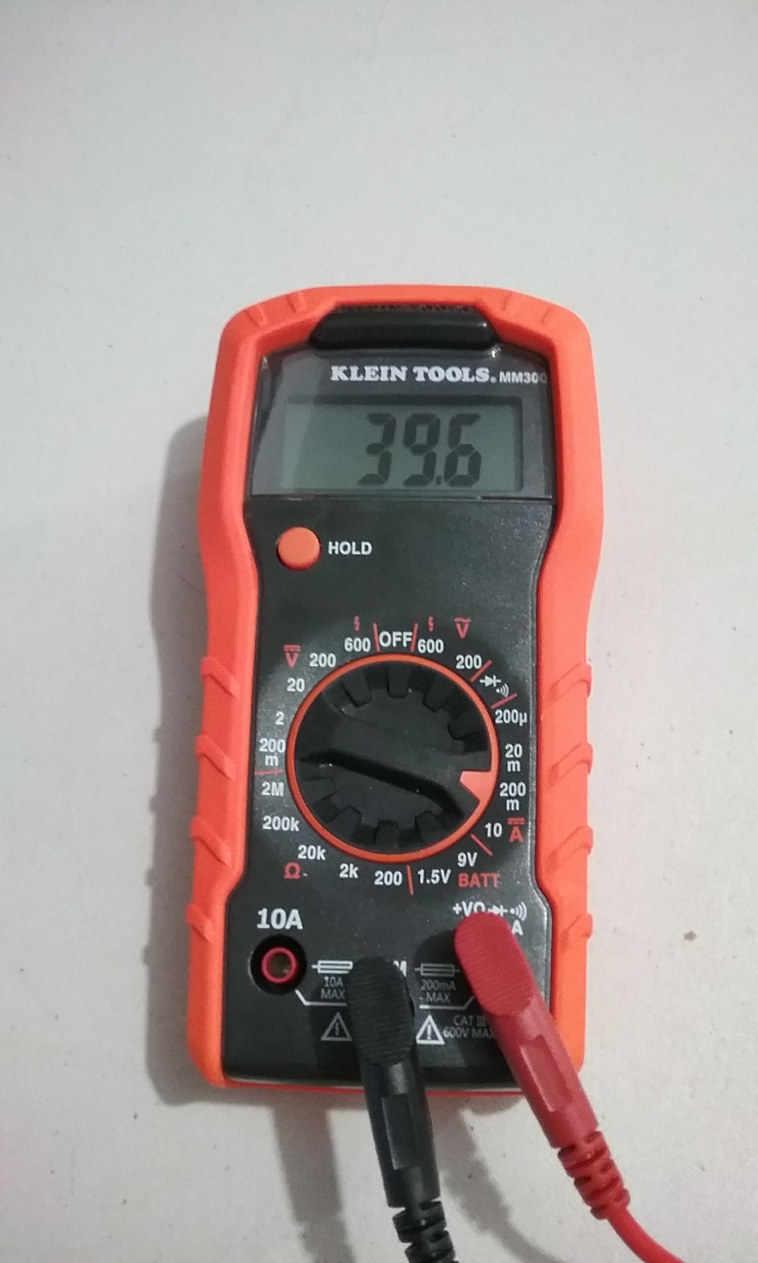
The power consumption is approximately 40mA:
![]()
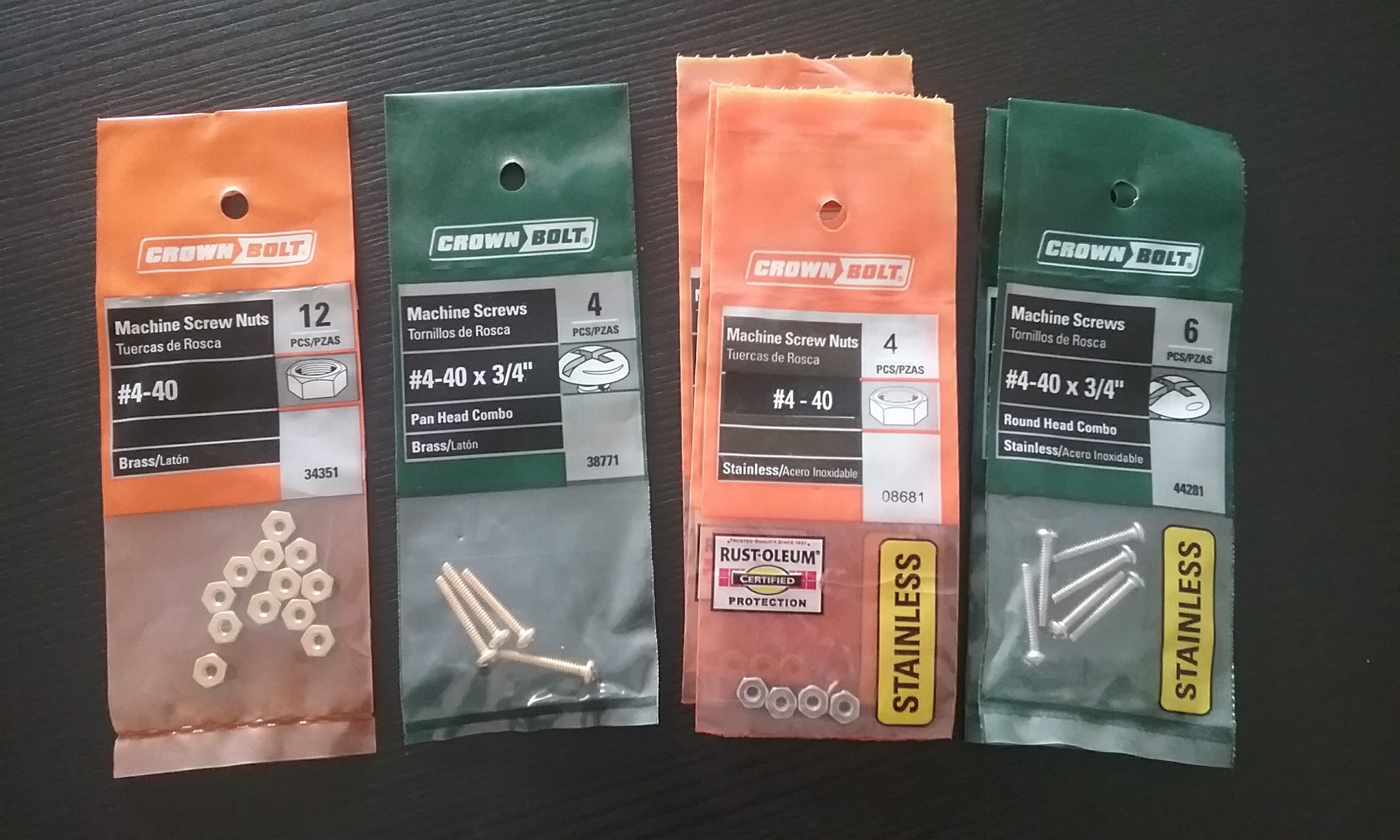
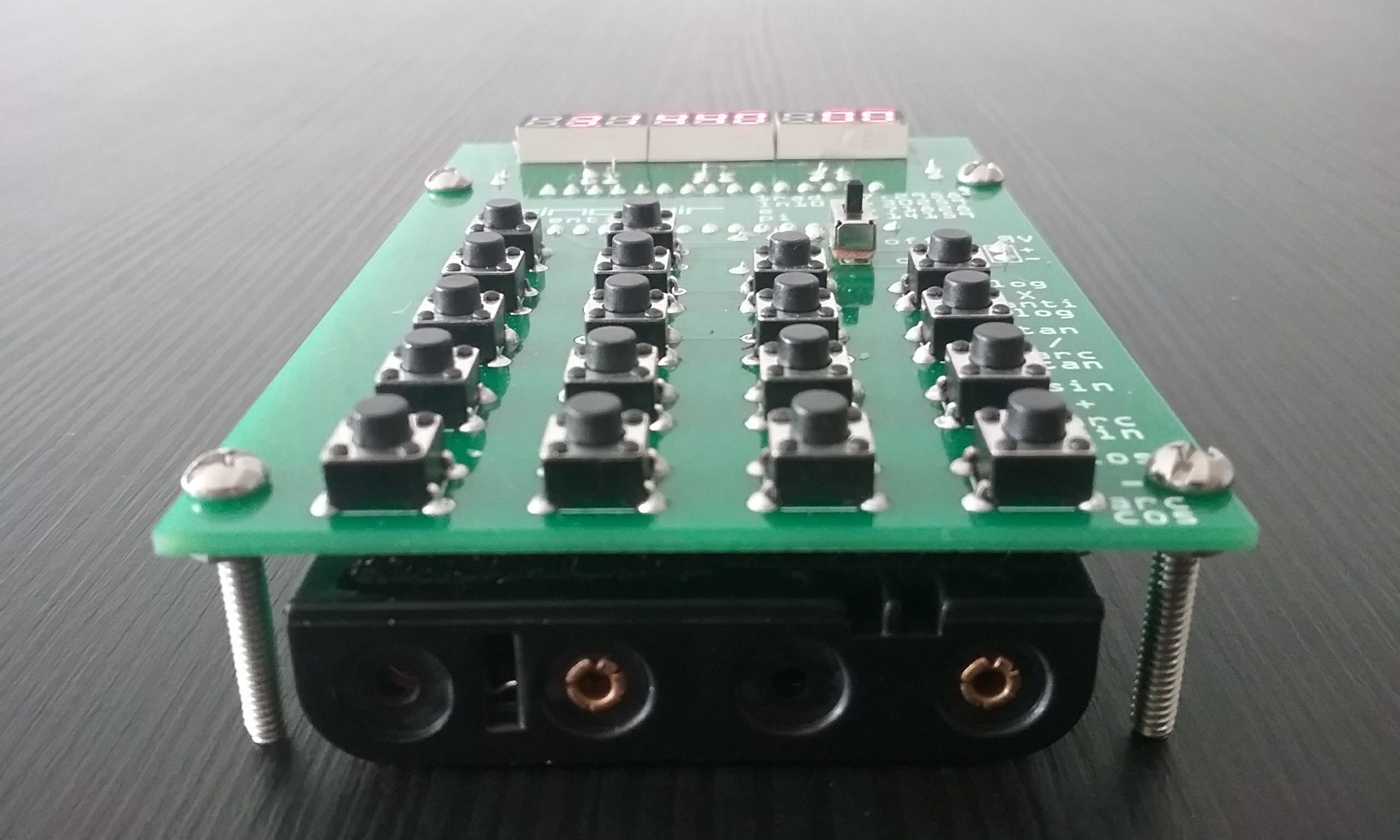
Standoffs are just #4 screws for the moment, later we will try to find plastic standoffs:
![]()
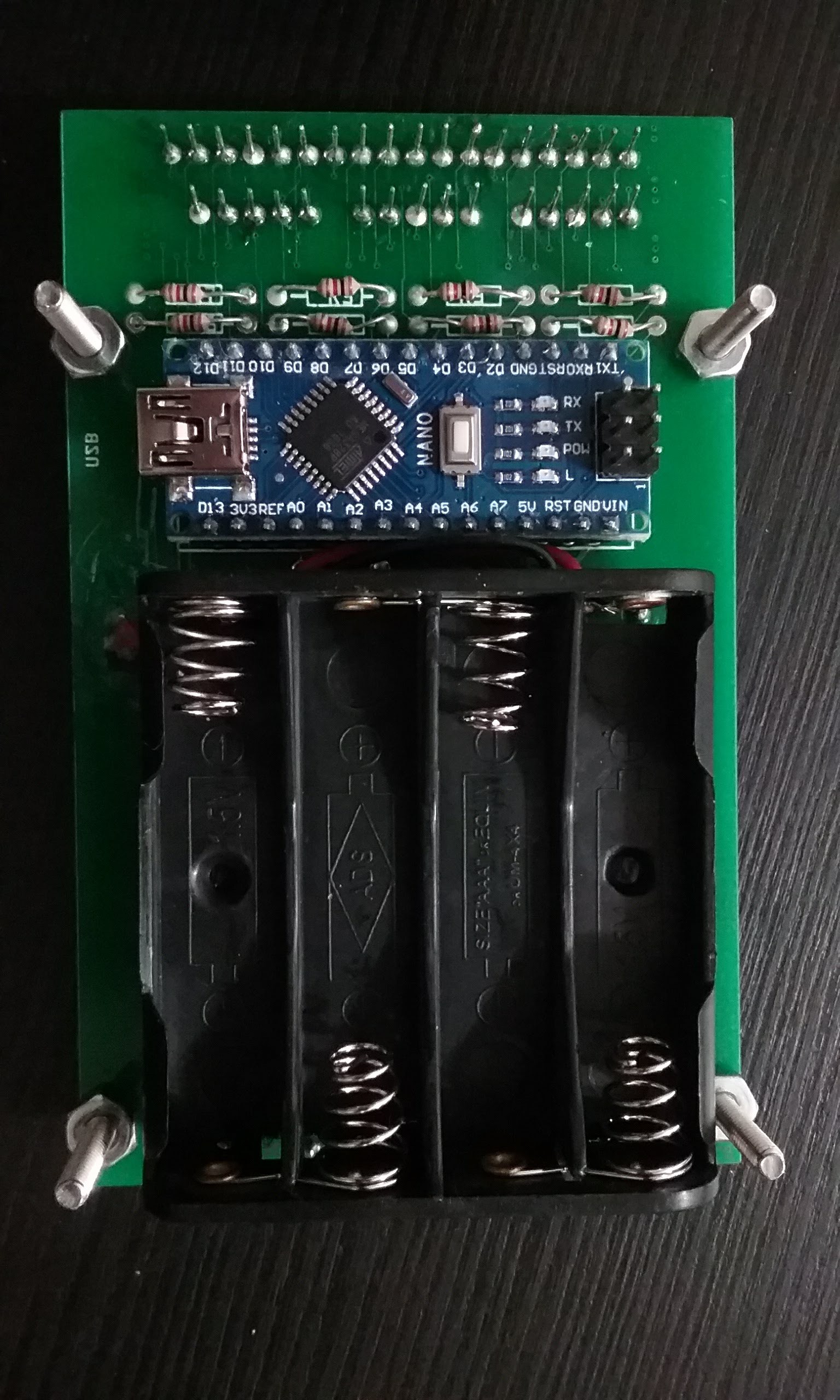
Everything mounted, the battery pack is attached with velcro that has been glued to the calculator:
![]()
![]()
Time for a quick instagram post:
-
01/14/2018 - All the display digits now work. At the cost of a Serial Port
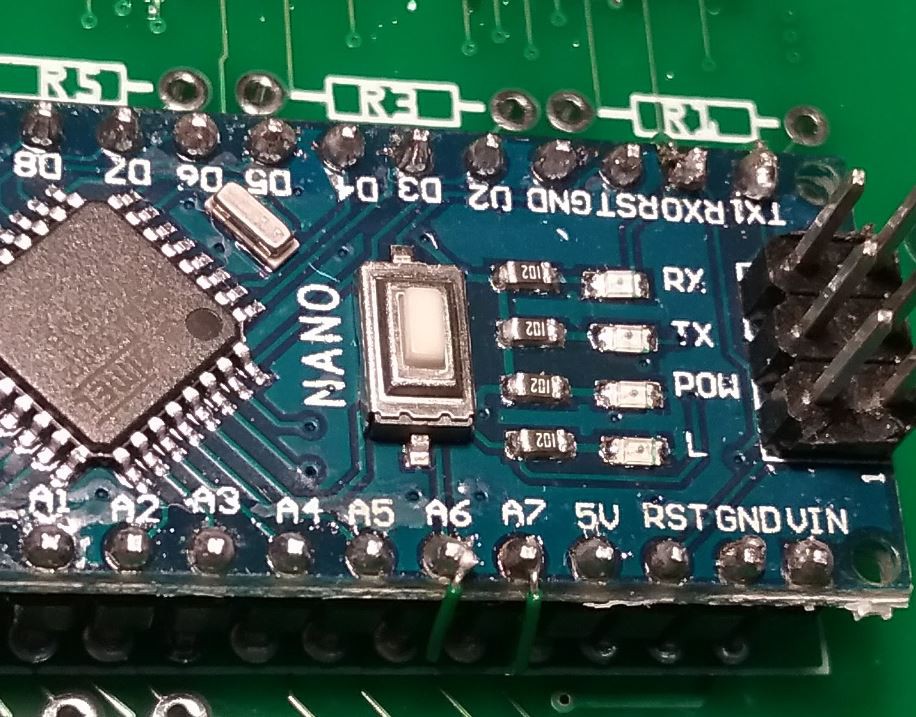
04/13/2018 at 04:32 • 0 commentsAfter much thinking, I decided to use the D0 and D1 pins to select the anodes of the first two digits. This will get me a working calculator, but the built in serial input / output will be compromised. Since the code is working and further debugging will be simple, this is a tradeoff I am willing to accept at the moment.
Since the A6 and A7 pins are inputs, they do not need to be disconnected. The quickest way to fix this is to bridge A0 to A6 and A1 to A7
In the following development prototype, this fix is done very visibly. The wires can be concealed on the back of the unit.
![]()
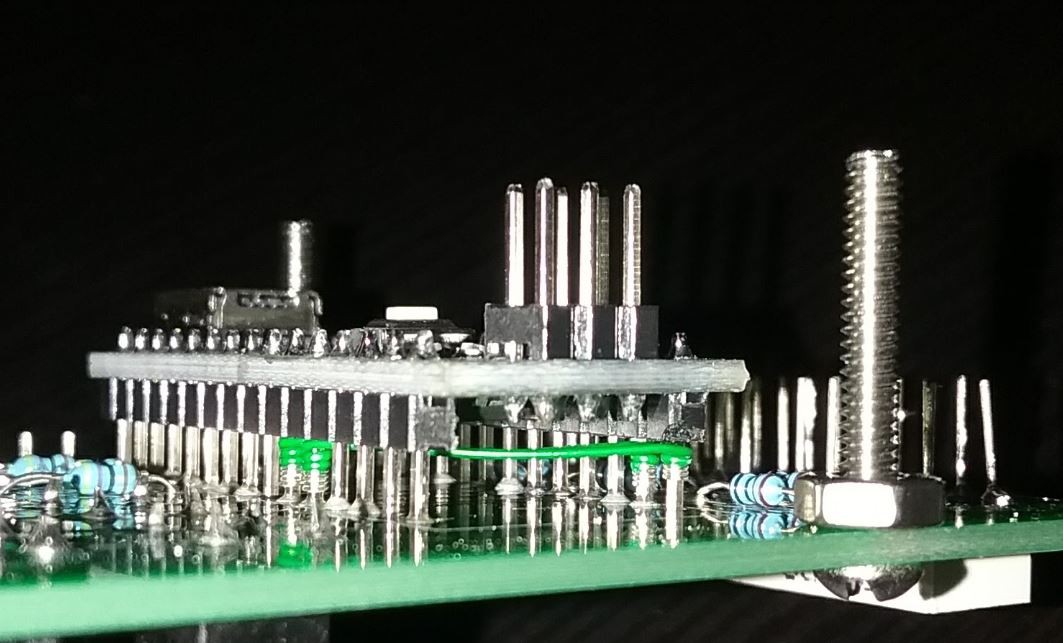
Green Wires soldered directly on the Arduino and wires routed underneath:
![]()
And finally wire wrap, the cleanest solution.
![]()
Here is the first video showing that all the digits work!
Time for a quick instagram post:
-
01/10/2018 - Input Output Working
03/23/2018 at 02:17 • 0 commentsAfter finding the definition of keys[] and figuring out how to make keystrokes visible to the CPU code, the simulator is now reading the keys. Since the first two digits are still not operational, they have been shifted two digits to the right. This is for the moment a 3 digits of precision calculator.
The following CPU code shows what needs to be done to simulate a keypress. The external code at the appropriate time must put the value KN on the keyStrobe. The appropriate time is decided by the value of dActive, a variable that holds the position of the digit currently being displayed.
case 26: // AKCN: A+K -> A until key down on N or D11 [sic]
        // Patent says sets condition if key down, but real behavior
        // is to set condition if addition overflows (i.e. no key down)
        //SinclairData.display = 0; //comment this line to glitch the display when a number key is pressed (SINCLAIR behavior: actual hardware behavior)
        add(SinclairData.a, getMask(), SinclairData.a);
        if (SinclairData.keyStrobe == KN)
        {
          displayInstruction(27);
          // Advance to next instruction
        }
        else if (SinclairData.dActive != 10)
        {
          displayInstruction(28);
          // Hold at current instruction and continue scan
          nextAddress = SinclairData.address;
        }
        else
        {
          displayInstruction(29);
          // For state d10, fall through
        }
        break;
Here are the key definitions. Each column corresponds to a dActive value of 1 to 10. To simulate that the key 3 is pressed, the external code must wait for dActive == 3 and then set keyStrobe to KN. To simulate a 0, wait for dActive == 9 and then set keyStrobe to KO
const char keysKN[10] = {'1', '2', '3', '4', '5', '6', '7', '8', '9', 0};
const char keysKO[10] = {'C', 'v', '+', '-', '/', 'X', '^', 'E', '0', 0};
//const char keysKP[10] = {0, 0, 0, 0, 0, 0, 0, 0, 0, 0};
Time for a quick tweet:
-
01/08/2018 - Simulator Works
03/23/2018 at 02:16 • 0 commentsAfter porting all of the CPU functions, the original Sinclair code starts executing in its Arduino host. It stays in a loop waiting for a key to be pressed. This is not implemented yet.
If you look closely, the terminal window says this code is running on an Arduino Uno. For coding experiments, I tend to grab the closest available Enigma Machine Simulator that is laying around on my desk.
![]()
Time for a quick tweet: -
01/07/2018 - Using a fast pin library to improve performance
03/23/2018 at 02:09 • 0 commentsIf you care at all about performance, the Arduino built in pin output function (digitalWrite) is not fast enough. Luckily, many fast IO implementations exist. I am using this one:
https://github.com/mikaelpatel/Arduino-GPIO
https://github.com/mikaelpatel/Arduino-GPIO/blob/master/src/Hardware/AVR/GPIO.h
The pins have to be declared as individual objects, which looks scary at first, but a display function can be created to display any number on any position.
GPIO<BOARD::D5>  SegmentA;
GPIO<BOARD::D8>  SegmentB;
GPIO<BOARD::D10> SegmentC;
GPIO<BOARD::D19> SegmentD;
GPIO<BOARD::D9>  SegmentE;
GPIO<BOARD::D6>  SegmentF;
GPIO<BOARD::D14> SegmentG;
GPIO<BOARD::D18> SegmentDP;

GPIO<BOARD::D2>  Digit1;
GPIO<BOARD::D3>  Digit2;
GPIO<BOARD::D4>  Digit3;
GPIO<BOARD::D17> Digit4;
GPIO<BOARD::D16> Digit5;
GPIO<BOARD::D7>  Digit6;
GPIO<BOARD::D15> Digit7;
GPIO<BOARD::D11> Digit8;
GPIO<BOARD::D12> Digit9;
The pins are initialized in the following functions:
void allSegmentOutput() {
  SegmentA.output();
  SegmentB.output();
  SegmentC.output();
  SegmentD.output();
  SegmentE.output();
  SegmentF.output();
  SegmentG.output();
  SegmentDP.output();
}

void allSegmentOff() {
  SegmentA.high();
  SegmentB.high();
  SegmentC.high();
  SegmentD.high();
  SegmentE.high();
  SegmentF.high();
  SegmentG.high();
  SegmentDP.high();
}

void allDigitOutput() {
  Digit1.output();
  Digit2.output();
  Digit3.output();
  Digit4.output();
  Digit5.output();
  Digit6.output();
  Digit7.output();
  Digit8.output();
  Digit9.output();
}

void allDigitOff() {
  Digit1.low();
  Digit2.low();
  Digit3.low();
  Digit4.low();
  Digit5.low();
  Digit6.low();
  Digit7.low();
  Digit8.low();
  Digit9.low();
}
To use them, call outputDigit to put the correct bits for a number in the bus, then call selectDigit to activate the correct anode.
byte outputDigit(signed char digit, bool decimalpoint = false) { byte segmentslit = 0; allDigitOff(); if (decimalpoint) { segmentslit++; SegmentDP.low(); } else { SegmentDP.high(); } switch (digit) { case 0: SegmentA.low(); SegmentB.low(); SegmentC.low(); SegmentD.low(); SegmentE.low(); SegmentF.low(); SegmentG.high(); segmentslit += 6; break; case 1: SegmentA.high(); SegmentB.low(); SegmentC.low(); SegmentD.high(); SegmentE.high(); SegmentF.high(); SegmentG.high(); segmentslit += 2; break; case 2: SegmentA.low(); SegmentB.low(); SegmentC.high(); SegmentD.low(); SegmentE.low(); SegmentF.high(); SegmentG.low(); segmentslit += 5; break; case 3: SegmentA.low(); SegmentB.low(); SegmentC.low(); SegmentD.low(); SegmentE.high(); SegmentF.high(); SegmentG.low(); segmentslit += 5; break; case 4: SegmentA.high(); SegmentB.low(); SegmentC.low(); SegmentD.high(); SegmentE.high(); SegmentF.low(); SegmentG.low(); segmentslit += 4; break; case 5: SegmentA.low(); SegmentB.high(); SegmentC.low(); SegmentD.low(); SegmentE.high(); SegmentF.low(); SegmentG.low(); segmentslit += 5; break; case 6: SegmentA.low(); SegmentB.high(); SegmentC.low(); SegmentD.low(); SegmentE.low(); SegmentF.low(); SegmentG.low(); segmentslit += 6; break; case 7: SegmentA.low(); SegmentB.low(); SegmentC.low(); SegmentD.high(); SegmentE.high(); SegmentF.high(); SegmentG.high(); segmentslit += 3; break; case 8: SegmentA.low(); SegmentB.low(); SegmentC.low(); SegmentD.low(); SegmentE.low(); SegmentF.low(); SegmentG.low(); segmentslit += 7; break; case 9: SegmentA.low(); SegmentB.low(); SegmentC.low(); SegmentD.high(); SegmentE.high(); SegmentF.low(); SegmentG.low(); break; segmentslit += 5; case 10: SegmentA.high(); SegmentB.high(); SegmentC.high(); SegmentD.high(); SegmentE.high(); SegmentF.high(); SegmentG.low(); segmentslit += 1; break; case 99: SegmentA.high(); SegmentB.high(); SegmentC.high(); SegmentD.high(); SegmentE.high(); SegmentF.high(); SegmentG.high(); break; default: allSegmentOff(); break; } return segmentslit; } byte lastSelectDigit = 0; void selectDigit(byte digit) { lastSelectDigit = digit; allDigitOff(); allDigitInput(); switch (digit) { case 1: Digit1.high(); Digit1.output(); break; case 2: Digit2.high(); Digit2.output(); break; case 3: Digit3.high(); Digit3.output(); break; case 4: Digit4.high(); Digit4.output(); break; case 5: Digit5.high(); Digit5.output(); break; case 6: Digit6.high(); Digit6.output(); break; case 7: Digit7.high(); Digit7.output(); break; case 8: Digit8.high(); Digit8.output(); break; case 9: Digit9.high(); Digit9.output(); break; } } -
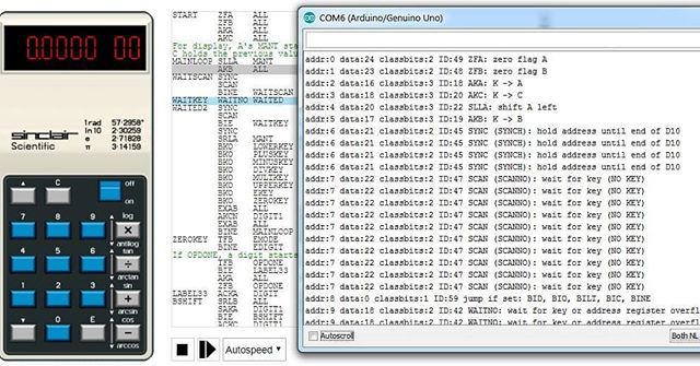
01/06/2018 - Work on the Arduino port of the TMS0805 Simulator continues
03/22/2018 at 20:07 • 0 commentsWe start the process of porting righto.com/sinclair to an Arduino sketch by looking under the hood.
![]()
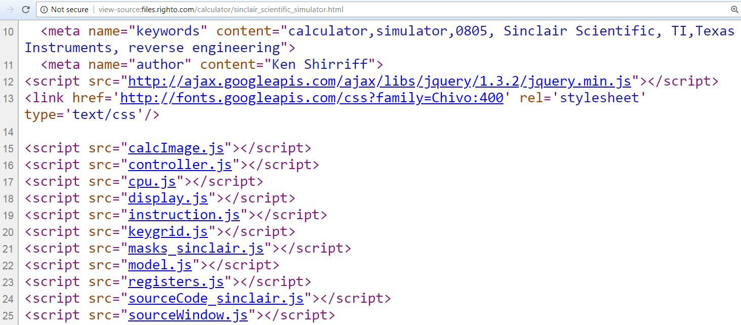
Right click on an empty place on the page and select View page source. This is a very friendly page that is meant to be read and understood by others. We have to start finding out what happens in each of the following modules.
![]()
The file cpu.js is important to us, so are masks_sinclair.js, model.js, sourceCode_Sinclair.js
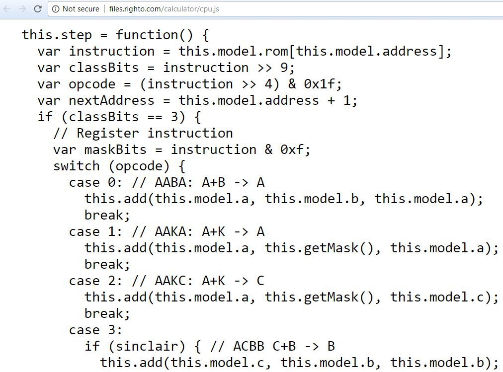
Here is the beginning of the CPU step function, found in CPU.js
We have to start looking for important functions and their dependencies. The function step() seems important, it fetches an instruction, decodes and executes it. it depends on variable called model and it uses extensively a function called add.
![]()
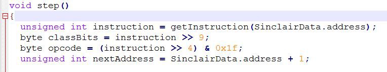
Javascript programs look like C, but it is not a strong typed language. Porting this code involves determining what the proper C type will be to replace the var declaration in Javascript. One has to find out if the value is 16 bits, 8 bits, positive values only or can it go negative.
Below is the ported code. Since the instructions are numbers greater than 255, but less than 65535, and they are always positive, the type unsigned int (we could also use uint16_t). The variables classBits and opcode are bit shifts of the variable instruction. Looking at the amount of shifts or the mask applied with a bitwise AND (&) operator, one can see that these hold 8 bit values and can be expressed as byte or uint8_t.
![]()
Looking at the add function we see that it depends on getMask and maskVec, time to find those functions and port them.
![]()
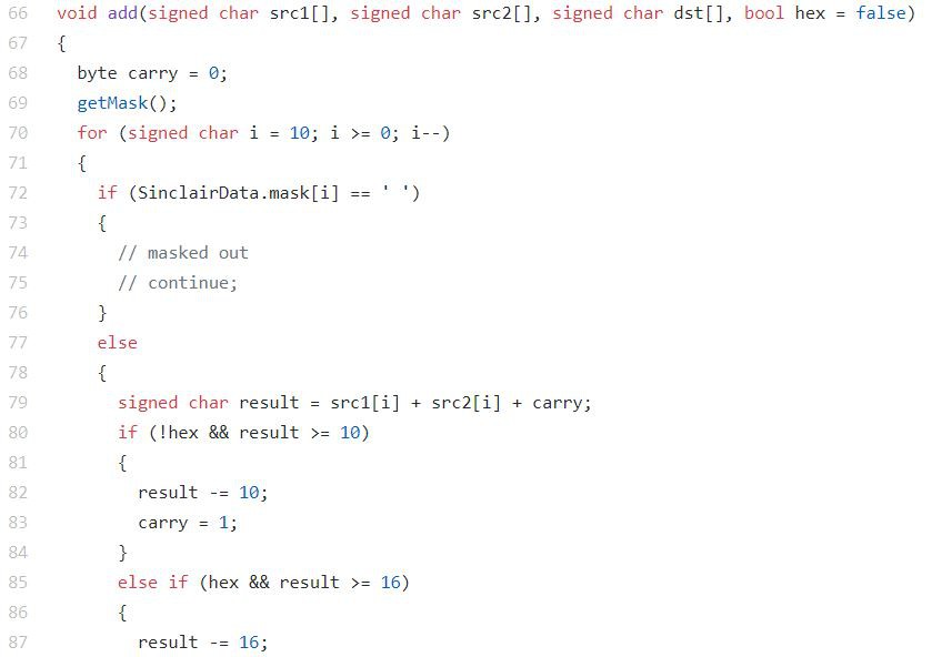
As a quick example of the effort involved, here is the C version of this function. The amount of information that has to be added is visible. Since src1 is an array of 8 bit values that can go negative, signed char src1[] is used. The for loop logic counts down from 10 to 0, exiting when it goes negative, a signed char has to be used here as well.
![]()
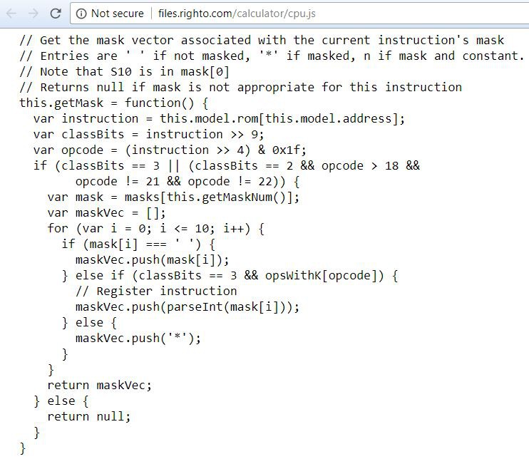
The mask function is also found in cpu.js. We need to identify its dependencies and the data types of the variables used.
![]()
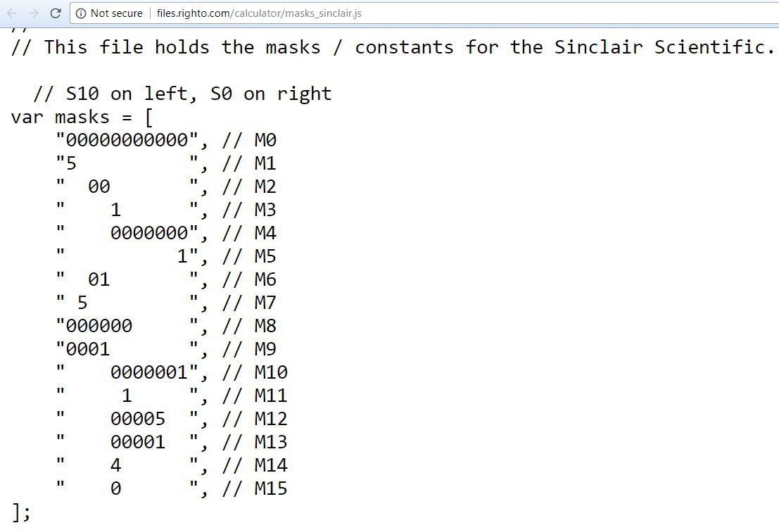
Here are the masks, expressed as an array of strings. Since this do not change, when porting these, the keyword PROGMEM will be used to keep them in ROM space in the Arduino and not load them into the very limited 2K RAM space. The pgm_read_byte_near() function is needed to get their values from ROM.
![]()
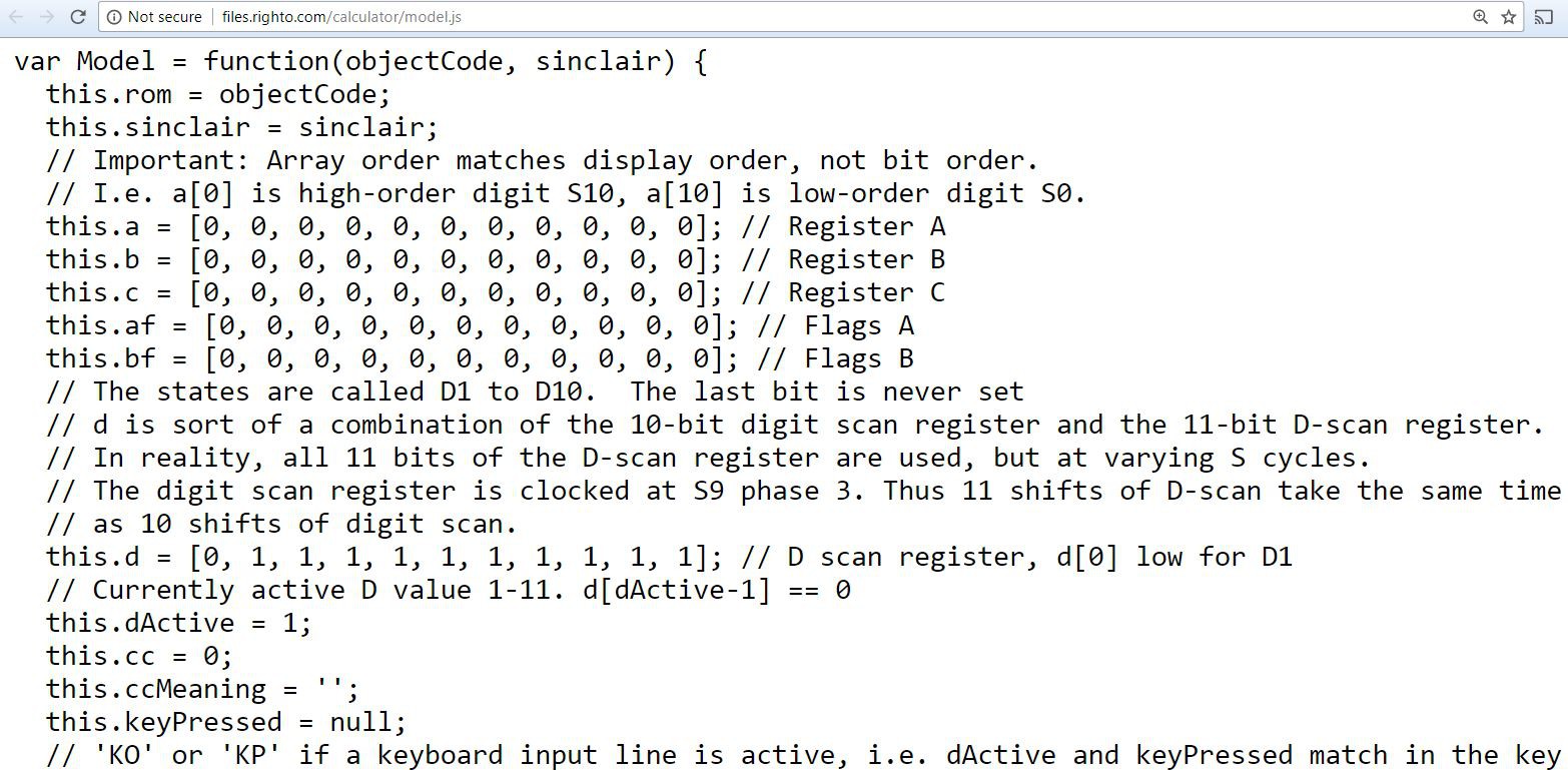
Here is an important data structure. It holds all the CPU registers, flags, program counter,
![]()
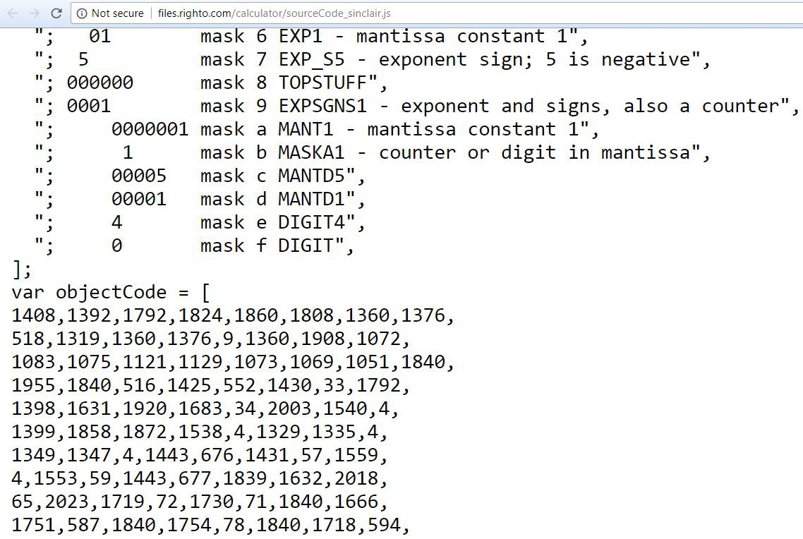
Finally, the actual original Sinclair program can be found in the objectCode variable. Above it is a commented disassembly of the program.
![]()
To put things in perspective, here is the whole program for the Sinclair Scientific Calculator. The rest of the Javascript files decode, execute, and interface these 320 instructions to the real world.
![]()
This was bothering me for a while. I could not find the definition of the keys[] array in any of the Javascript files. It turns out it was in the main webpage.
![]()
The following file is the beginning of the porting efforts. It contains the ALU (Arithmetic Logic Unic) functions such as ADD, SUB, COMPARE and their mask related dependencies. The setup function tests those functions and displays the results.
Here is the final Arduino Sketch (SinclairScientific1.ino). It has all the data structures needed by the CPU emulator. Everything is put together here, the keyboard is read, the display updated and the CPU stepped.
The code for the CPU emulator is here. These links open in a new window so you can see the Javascript code above and find the equivalent C functions and see how they were translated.
The following file is called by the step() function with a sequential instruction ID number assigned to each original cpu instruction. It was useful at the beginning to see that the instructions being executed matched the disassembly on the web page.
Time for a couple of Tweets:
https://twitter.com/arduinoenigma/status/947907337016283138
![]()
https://twitter.com/arduinoenigma/status/948018715924357120
![]()
-
01/05/2018 - V1 is assembled, a problem appears
03/22/2018 at 01:06 • 0 commentsAfter soldering all the components and writing a test program to display 012345678, we notice something bad. The first two digits are off. Nothing we try in software changes that, they do not want to light up at all.
![]()
And this is how we find out A6 and A7 are input only. They are the selection lines for the first two digits. They need to supply 5V and cannot do so.
![]()
Also, the multiplexing algorithm is wrong, 8 is brighter
Time for a quick instagram post while we think how to get out of this mess.
-
01/03/2018 - The manufactured V1 boards arrive
03/22/2018 at 00:56 • 0 commentsThe manufactured boards arrive and they are beautiful. Holding in your hand something that prior to this only existed in a computer screen is a nice feeling.
Here is a picture of the front and a comparison to a printout of the prototype from prior log. The footprint for the Arduino Nano is correct, one has been temporarily inserted just to do a test fit.
![]()
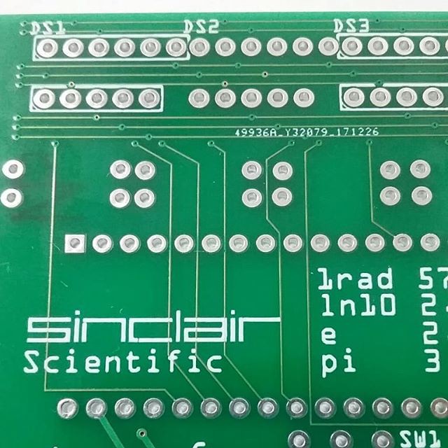
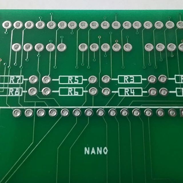
Some details of the front, traces are 8 mil, the fab house has no problem running them in between the solder pads for the Arduino Nano. Next time, we need to pay attention to not running traces through logos in the front of the board.
On the next revision, we need to either relocate the DS1 DS2 and DS3 labels under the display or delete them completely. The manufacturer also added their PCB ID tag in a space between the display bus bars, but since it is outside the display footprint, it will be visible. We need to provide a rectangular area under the displays for the manufacturer to place their board identification number.
The label SW1 on the switch also needs to go under the switch or away. The label 9V needs to be moved to the back, where the power cable will come in.
![]()
details of the back:
![]()
Today is a good day. Time for a quick instagram post:
-
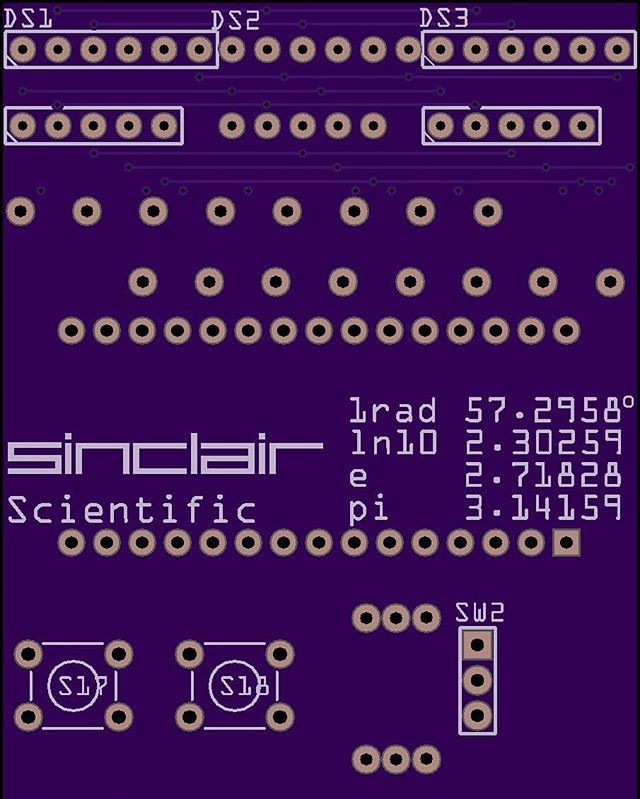
12/30/2017 - The desire to design a slimmer version begins
03/21/2018 at 21:42 • 0 commentsWhile waiting for the V1 PCB to come back from the fab, I play with the concept of designing a slimmer version. Since the original calculator is 110mm x 50mm, to have the same proportions in a 100mm board, the width would have to be 46mm.
Each display is 15mm wide, all three would take 45mm, so this seems plausible. The display resistors are tentatively arranged in a 45 degree angle.
![]()
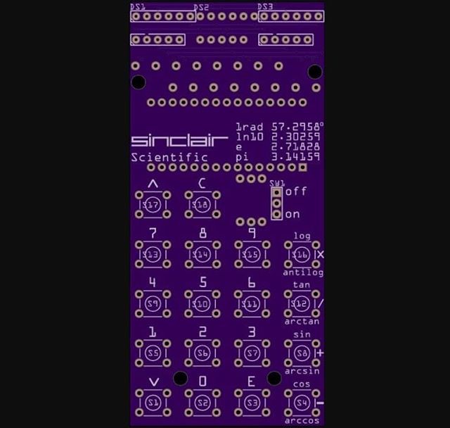
An attempt is made to have the separation between the displays and the keyboard resemble the actual calculator. The key spacing in the X and Y dimensions is also calculated to match the look of the original.
![]()
In the end, this is only a proof of concept that is never fully routed or sent to production. I wanted to wait until the first version is up and running to find out where the problems will be before designing another board. This proves to be a good decision.
Retrospectively, here are the problems this board was going to run into:
1) A battery holder for 4 AAA batteries is at a minimum 48-49mm wide. The board needs to be at least this width to conceal it in the back. The original calculator uses some surface mount battery contacts that I have not been able to find a satisfactory replacement for.
2) The holes for the bottom standoffs were placed above the bottom row of keys since there is no space below the keys. I do not realize this now, but this space will be taken by the battery holder. The holes for the lower standoffs must be at the bottom of the board.
3) I still don't know about the A7/A6 pins being input only, so this would be wired like the first version boards and thus require a green wire fix.
4) To get the proper separation between the display and the keys, the board needs to be 110mm tall. If a design is kept under 100mm x 100mm, it could be fabricated for $2 for 10 boards. Shipping costs would be $8 for regular and $17 for express. Manufacturing this board using the proper White soldermask negates this price advantage, at that moment, it is not a huge cost increase to design a 110mm x 50mm.
This design is put in the refrigerator until V1 is up and running.
Time for a couple of quick instagram posts:
-
12/25/2017 - Finished Routing the Board and Submited for Production
03/19/2018 at 20:07 • 0 commentsThe Gerber files for this version can be downloaded here:
https://oshpark.com/shared_projects/HpVh3N0L
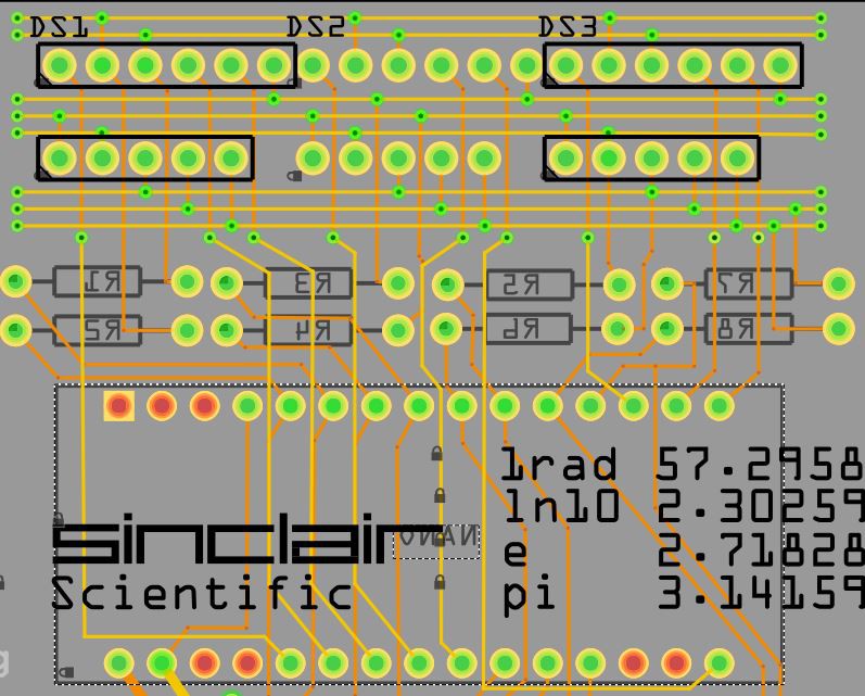
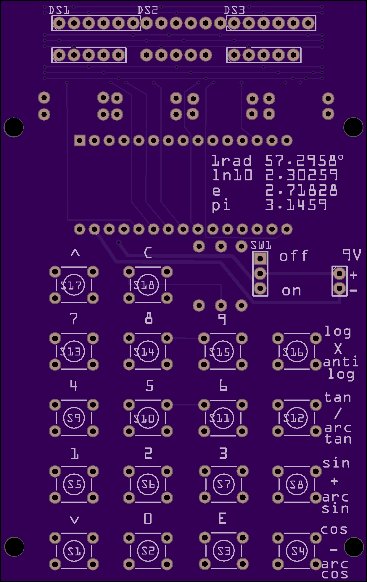
The remaining connections from the Arduino Nano to the current limiting resistors, the LED display common anodes, and the keyboard lines have been routed.
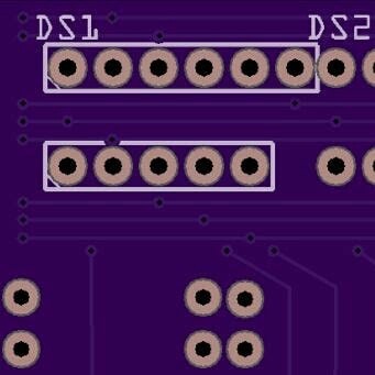
Since there are vias everywhere, connecting a via to an arduino pin is not particularly difficult if both layers are used and one is not picky about which particular pin to use. Lighting up the correct digits will be done in software later. What I did not know at the time is that the A7 and A6 pins are input only. The A7 pin ended up being used to select digit 1 on the left most display. You can see the wire running through the S in the Sinclair LOGO to a via under DS1. Pin A6 was used to select digit 2 on DS1, it runs through the f in the word Scientific. All of the Arduino Nano I/O pins were used except for D0/RX and D1/TX
The vias at the end of the horizontal bus bars on the display are at this point there just for aesthetic purposes. On the keyboard part of the layout, deleting them allowed for the design to be optimized and mostly run on the back side of the board.
8 I/O pins: Connected to one side of the current limiting resistors (output). Connected to the return lines on the keyboard (input).
9 pins: used to drive the common anode of the LED displays (output). Displays the selected character formed by the 8 I/O lines in the desired position.
3 pins: Keyboard row selection (output). Used to select a row of switches, if a switch is pressed, it will be read as low on one of the 8 I/O pins used to drive the display. The internal pull up resistor on the Nano is enabled during this operation to allow the key presses to be read as low.
This design uses 20 pins. The nano has 22 I/O pins (of those A6/A7 are input only).
![]()
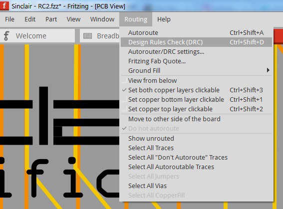
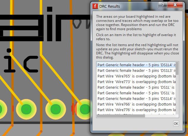
Before submitting anything, run the DRC (Design Rules Check) to ensure all traces are sufficiently separated.
![]()
Here are three traces passing in between pins. The one in the center is sufficiently separated from both pins. The one on the left shows a little red where it gets a little close to a pin. Sometimes, even with the align to grid feature turned off so that things can be moved very precisely, it is impossible to get the trace completely away from the pin, the red mark will move from the right side to the left side when the trace is moved a minute distance. In that case, its ok to leave as is. The track on the right is way too close to the pin, there is red everywhere. That one needs to be fixed.
![]()
Finally, it time to export the gerbers and upload to Oshpark.
Here is a rendering of the PCB Front:
![]()
Oshpark rendering of the PCB Back:
![]()
These are production boards, so a couple of extra steps are needed to place soldermask over the vias (tented vias). Two Gerber exports are going to be made, one with a full board, the other for the same board with the vias deleted. Each export goes into a different folder. Luckily, Fritzing supports an easy way to select all the vias. Save your work prior to deleting the vias and then revert to the saved file after the Gerber export is completed.
Once the two set of Gerber files are created, the soldermask files, and if desired, the sikscreen files from the no-vias folder can be copied to the vias folder. I have used this technique with multiple fab houses and it always works.
A default Gerber export will have exposed vias:
![]()
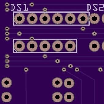
This is what Tented Vias look like. I did not copy the silkscreen file from the no-vias folder, so a discountinuity can be seen on the lower connector for DS1. By also copying the silkscreen file, a continuous line can be drawn over a via.
![]()
Fritzing Tips: Tented Vias
-Save Work
-File->Export->For Production->Extended Gerber, create "tented" folder
-Routing->Select All Vias
-Press Delete key
-Export Gerbers to no-vias folder
-File->Revert
-Copy maskTop and maskBottom files from no-vias to tented folder
Time for a quick instagram post:
Sinclair Scientific Calculator Emulator
A register level TMS0805 CPU emulator on an Arduino Nano runs the original 320 instruction calculator program. A custom PCB houses it all.