-
IO/65 Part #2
11/09/2017 at 13:33 • 0 commentsSo yeah, I now have a working 6502 mini cpu board but no IO... And still no crystal :S
And before I go on and build more modules, let me test this puppy out first.
![]()
This is my personal
doomsday device... TeensyIO, connected to the IO/65 CPU module ;)A breadboarded Teensy 3.1 running at 96MHz, a battery backed DS1307, 7segment led display and two MCP23017's for port extensions. With 64K ram, 256K program space and 32 additional pins, I can use this setup for almost everything. So in this case I use it to control the cpu and clock, and provide all "I/O" virtually.
In the current configuration, the DS1307 and led display are not connected to the I2C bus, since I'm not really using them. This allows me to crank up the I2C bus speed dramatically to 2.4MHz!!! Not that I will be needing the speed, since I am clocking the CPU at very slow rates (2Hz and up) so I can "see" what is going on.
The CPU is being fed with an Apple I memory map, with a virtual PIA for keyboard and display over the serial connection. At 2Hz it takes about a minute for the woz monitor to be ready for input.
Now I can focus on the memory map for this platform. I'll end up with several designs to allow for different setups to use. For the first usable design, I want to keep the part count as low as possible, while maintaining a moderate compatibility with existing designs.
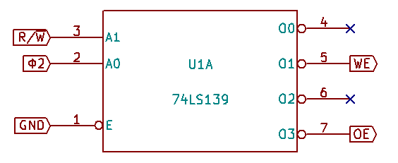
The first thing to focus on is providing separate OE/WE signals from R/W and PHI2. Most designs use a single inverter and two nand gates. After some careful consideration, I figured that one half of a 74xx139 2-to-4 decoder can do the job too.
![]()
With that out of the way, all that remains is filling in the gaps. The lower half of the map will be assigned to a single 32K block. And since we can use the other half of the decoder, we'll just split the upper half of the map into 8K blocks. This allows for a lot of flexibility on decoding the remaining blocks.
![]()
At this stage I have the decoding hardware down to 2 ic's: a 74xx04 and a 74xx139. I'll use the unused pins of the header to expose these signals to other modules.
I also realize I'm wasting 5 of the inverters on the 74xx04. On my first development version I think I'll just create the inverter in DTL and add 32K ram and 8K rom to save on parts.
See you soon in part #3 :)
-
IO/65 Part #1
11/09/2017 at 12:13 • 0 commentsA few years ago, I created a small project to get a NCR 65C02 running on a breadboard. A Teensy 2.0 was responsible for generating the cpu clock signal, while I was using a Teensy 3.1 as a ROM programmer. Inspired by the RC2014 project, I wanted to build something similar but based on the 6502.
![]()
So here's the basic design of the very first module.
![]()
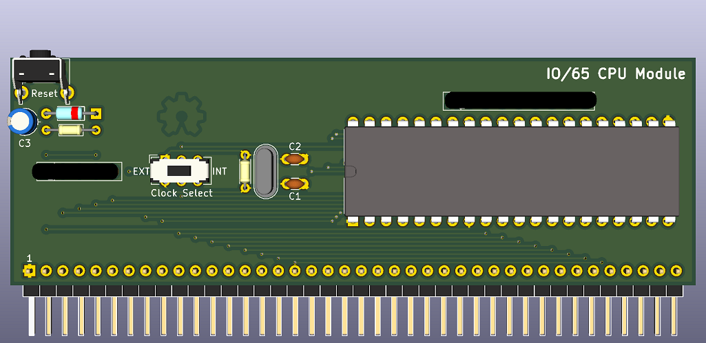
The circuit and board layout were made using KiCAD. It measures 105*35 mm, exposes most of the control signals, and provides standalone free-running when powered.
![]()
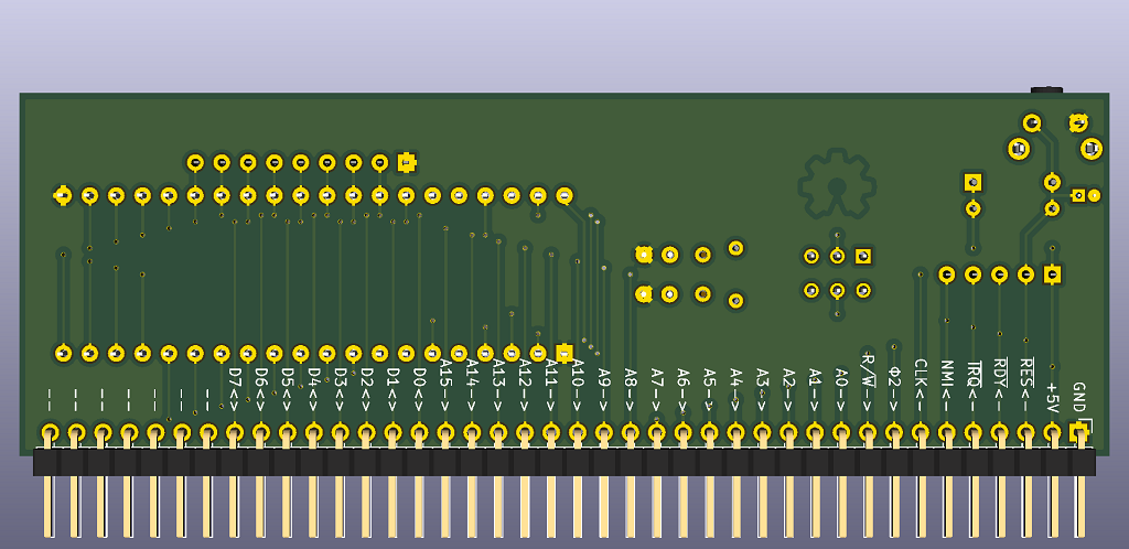
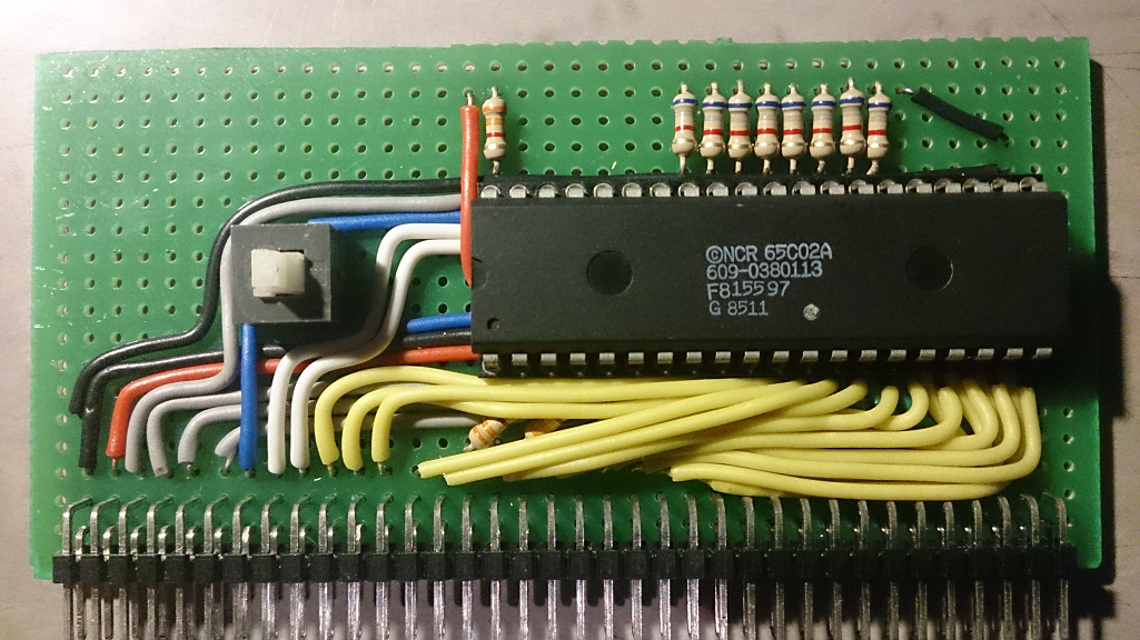
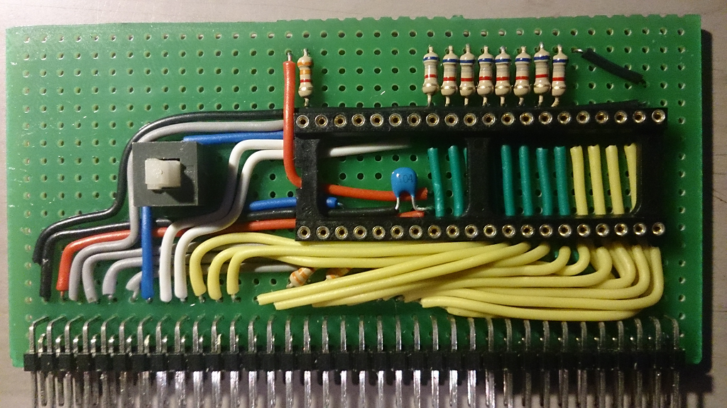
So this is what I ended up with. I excluded the reset button, and am using a 2*36 pin header instead. I did include the clock select switch, as I still don't have the required 1MHz crystal.
![]()
I probably shouldn't be running all them lines over and across each other. In hindsight, I could have exposed some additional pins. I did however use the exact same pinout as my initial design.
The change to the 36-pin header does have a reason. I wanted to build the initial backplane using a stripboard like this. And since I already have a few of these 2*36 angled headers and a set of female header rows, I'm good to go!
My initial tests proved the board was working as intended, with the cpu executing BRK (0x00) instructions forever.
See you in part #2 :)
My Pages
Projects I Like & Follow
Share this profile
ShareBits
Become a Hackaday.io Member
Create an account to leave a comment. Already have an account? Log In.
 djBo
djBo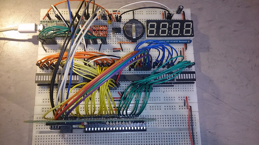

 davedarko
 Lukas Vacek
 StanleyProjects
 Tim Wilkinson
 Jorj Bauer
 Max2Play
 Todd
Todd Jakub Laník
 NaranInc
 Jacob Creedon
 Marcus Berg
 Ricardo Ferro
 ken.do