To measure the performance of the 555 oscillator we will primarily be looking at the Allan Deviation or 'ADEV'. Oscillator stability is a complex topic and there are much smarter people than me who can explain why ADEV is the measure of choice.
Establishing a Baseline
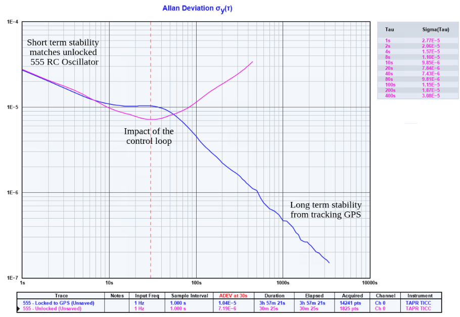
The first thing to do is capture the ADEV of the 555 RC oscillator when it is unlocked and not being controlled. This represents the base performance that we are looking to change via locking with GPS.
The 555 shows a 'U' shape that is very typical of nearly all oscillators.
The ADEV tells us that, on average, the 555 is counting every second with a variance of just 2.77E-5 (or 27 us).
It can do better though, if we measured the ticks over a 30 second period we can achieve a variance 7.19E-6. This is due to the averaging out of noise sources and is represented in the graph as the bottom of the 'U' shape.
However, if we measure over a longer period it actually gets worse and the variation starts to increase again. This is due to other noise sources, such as oscillator drift, becoming dominant. This is the right part of the graph.
GPS is Different
The PPS from a GPS receiver does not exhibit the same U shape as seen with an oscillator
It's actually just a straight line going down (ignoring a little wobble at the 4-5 second mark that is due to sawtooth).
The atomic clocks in GPS satellites are incredibly precise and any long term noise or drift with the clocks is corrected out. We can take the PPS output from a GPS receiver and look at it over longer and longer intervals and get increasingly lower variance, forever (or at least whilst GPS remains operational).
GPS Disciplining the 555
The aim of GPS disciplining an oscillator is to transfer that long term stability of the GPS signal to the oscillator, correcting the longer term noise sources that are present in the right hand side of the 'U' shape.
Here's how it did:
At short intervals, the stability matches that of the unlocked 555 RC oscillator.
The PIDs in the MCU have a maximum averaging window of 18 seconds (16 seconds average and a 2 second settling time after any change). Clearly visible in the ADEV results is a small degradation in the performance as the PIDs adjust the control voltage to lock to the GPS signal. This is the gap between unlocked (pink) and locked (blue) lines.
The unlocked ADEV shows that the minimum variance in RC oscillator is seen around intervals of 30 seconds. By extending the average time of the PID loops from 16 seconds to 30 we may be able to slightly improve the performance
At longer intervals the control loop is tracking the GPS PPS. The upturn in the 'U' seen in the unlocked oscillator is avoided and the variance continues to decrease with tau in a nice straight line.
Sucess !
The project succeeded at locking the 555 timer to GPS and achieving long term stability.
How Does it Compare to Other GPSDO ?
Badly.
This image shows the typical ADEV of various oscillators locked to GPS, it's borrowed from the SRS website.
Oscillators tend to have excellent short term performance, but poor long performance. On the other hand GPS has poor short term performance and excellent long term performance. The aim of a GPSDO is take an oscillator that performs better than GPS in the short term and get the best of both worlds, fusing the short term and long term performance.
The 555 RC Oscillator does not perform better than the GPS PPS
It's worse, a lot worse, in fact by locking the GPS to a 555 we're actually degrading the GPS PPS signal
It's not even close.
The one second pulse from the 555 has a deviation of 2.77E-5 meaning it wobbles around, on average, by 27us.
A standard GPS module has a deviation of around 4E-8 (GPS modules are often spec'ed to 42ns), which is 3 decades or approximately a thousand times better
A good OCXO or Rb standard will have a deviation under 1E-11, yet another 3 decades down and making them a million times better than the 555
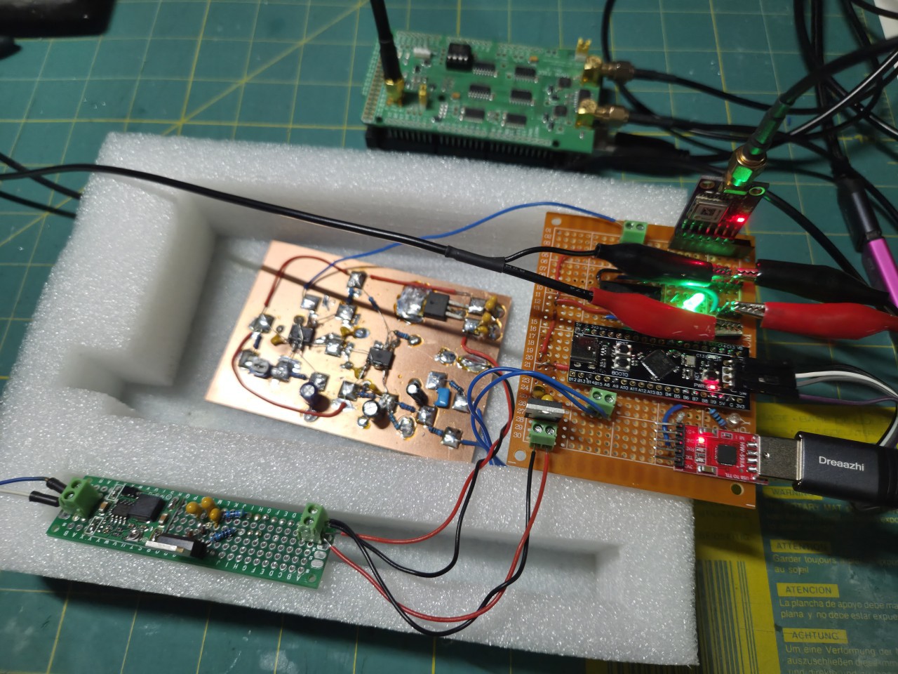
Time to see how well the boards perform against, well, time.
In another case of over doing it, here's the measurement set up.
The analogue board is placed in a foam box to protect against drafts that might cause short term temperature variations (Longer term temperature changes should be managed automatically by the control loop).
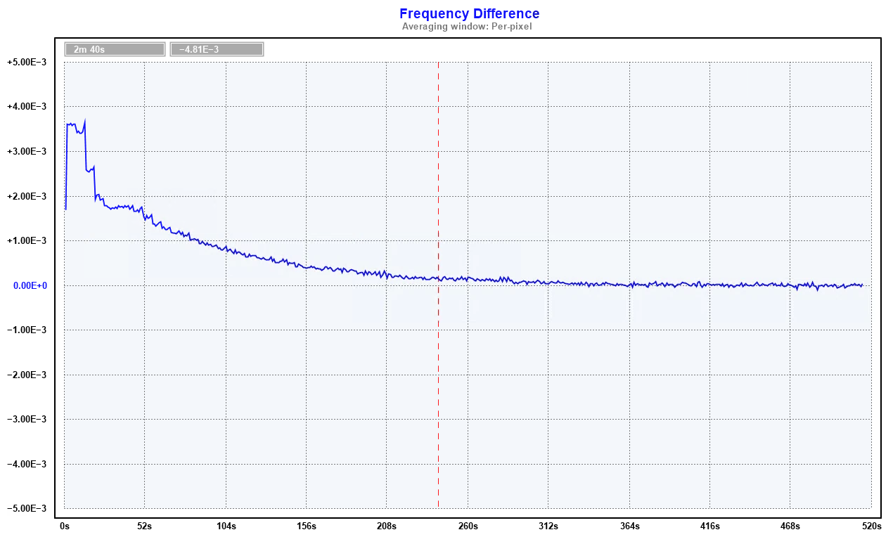
Frequency and Phase Lock
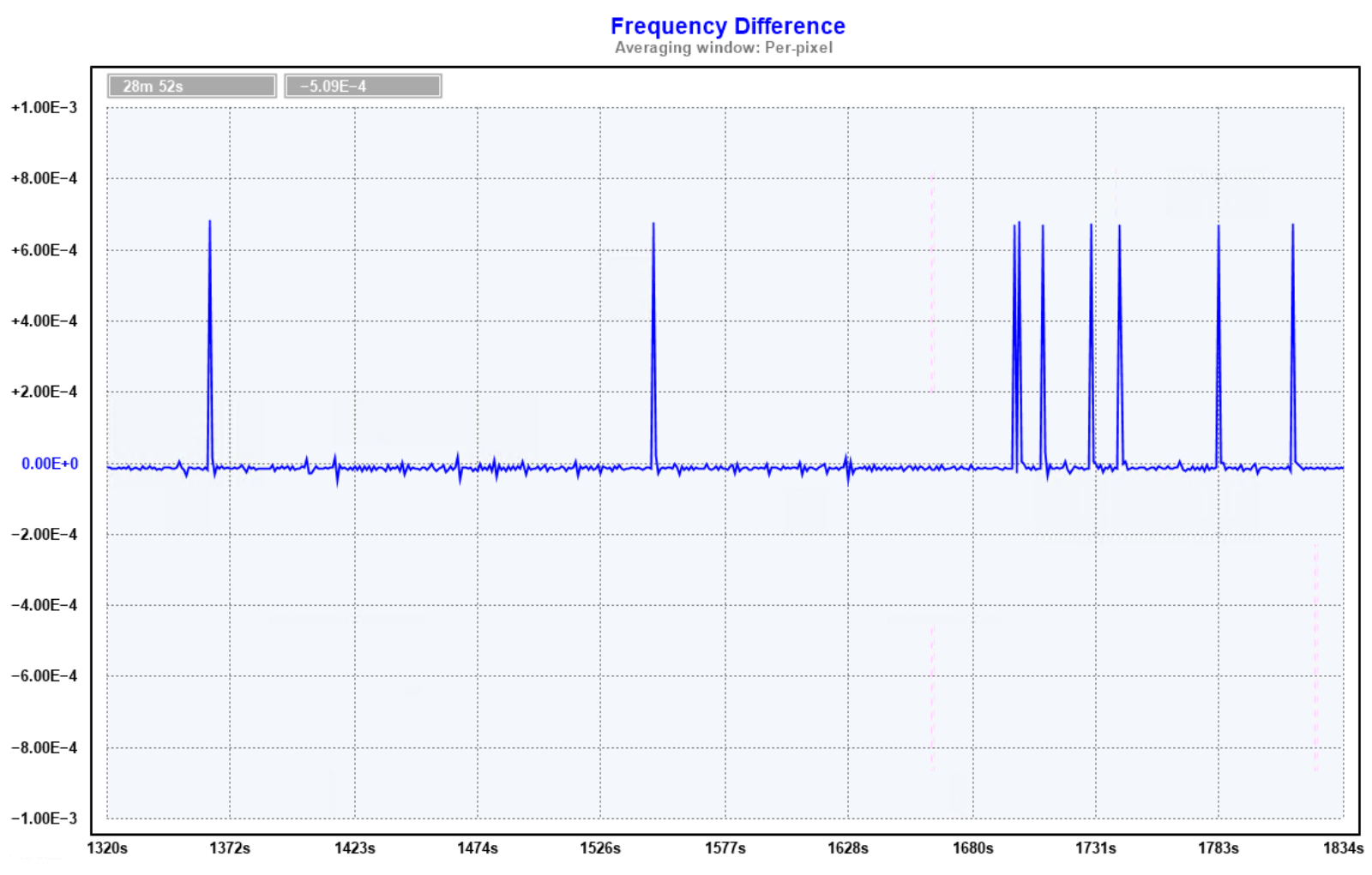
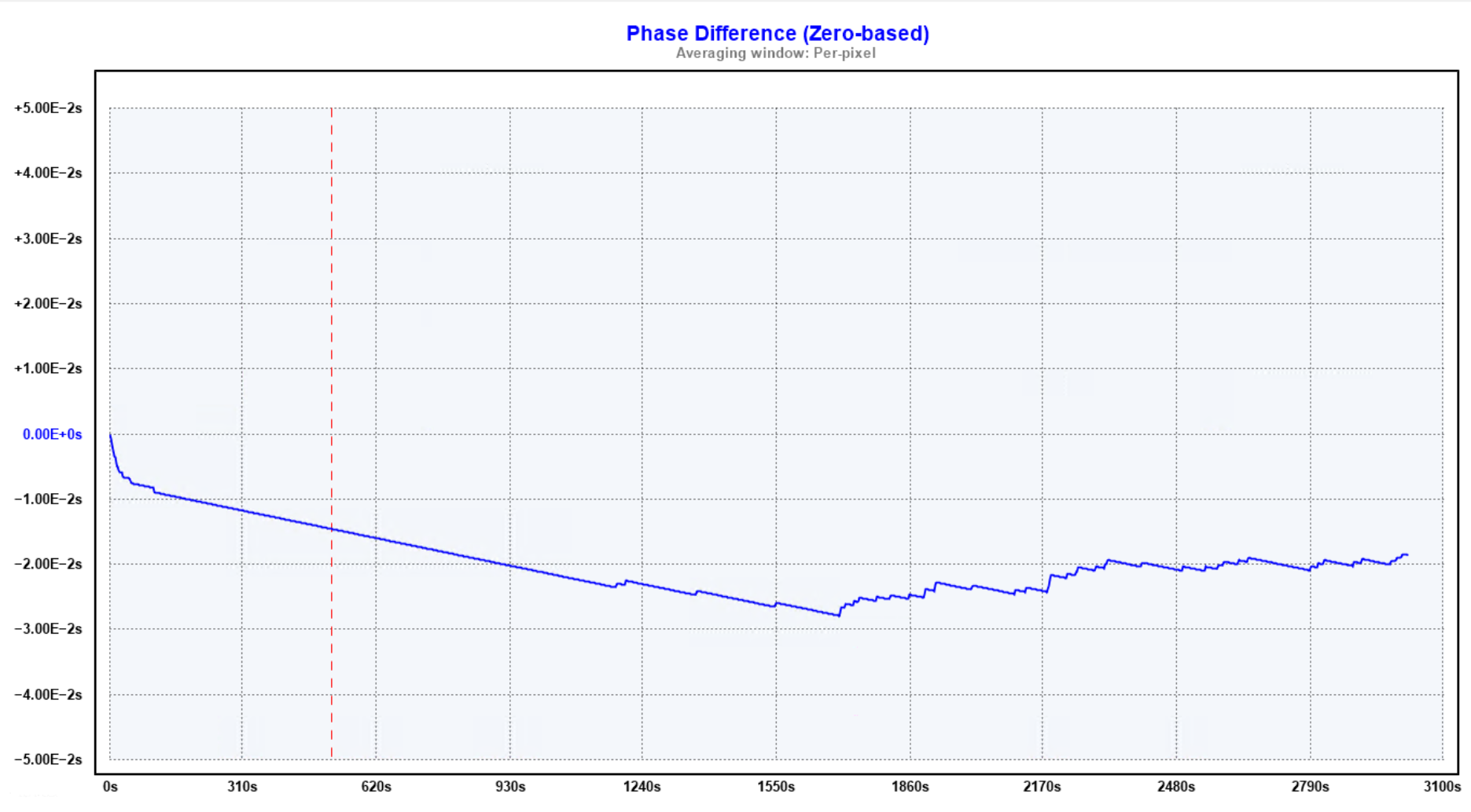
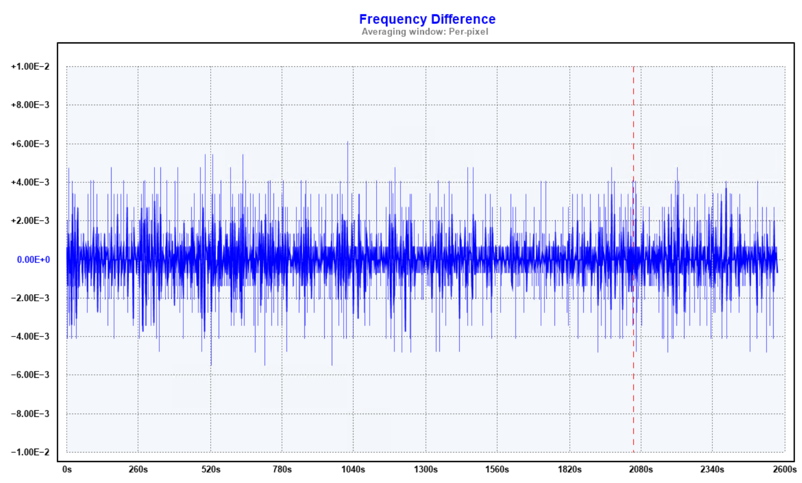
The following graphs show the frequency and phase difference of the 555 PPS against the GPS PPS following a reset.
Frequency offset
Phase offset
The control loop is slow, but this is a design choice and we are in no hurry.
The two PIDs are successfully able to bring both the frequency and phase in to alignment with the GPS PPS.
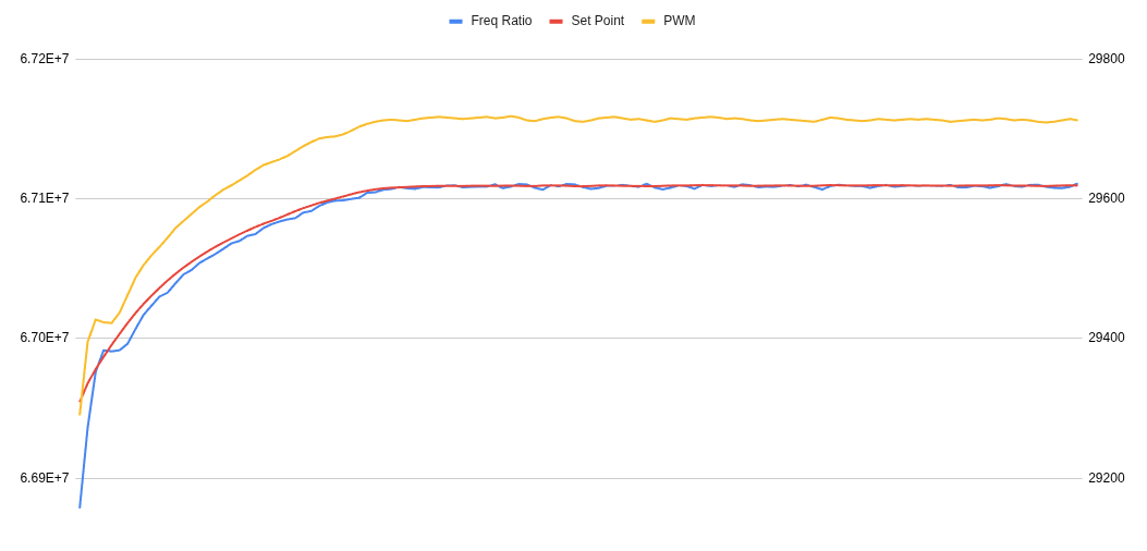
Here's the view from the MCU parameters.
The graph shows the frequency PID maintaining the blue line (measured frequency) against the red line (the frequency set point).
The curve of the red line (frequency set point) shows the phase PID adjusting the set point to drift the phase into phase lock.
Once locked, the phase is maintained with +/- 1 adjustments to the PWM. This hints that there may be slightly better performance available with smaller PWM steps and more control voltage resolution. The board under test has approximately 9uV per PWM step control voltage resolution.
With the analogue board completed, it's now time to build out the digital and power management sections.
Digital Section
The digital section is built on to standard perfboard, there's nothing much to see here other than marvel at the poor quality of the construction. At one point, I had power and ground backwards leading to some exciting choices but that's what happens when building out on the fly without a plan. Memo to self, draw a diagram first.
Breakout pins were added for ground and the PPS signals from the 555 and GPS; these facilitate connecting the TICC for doing measurements.
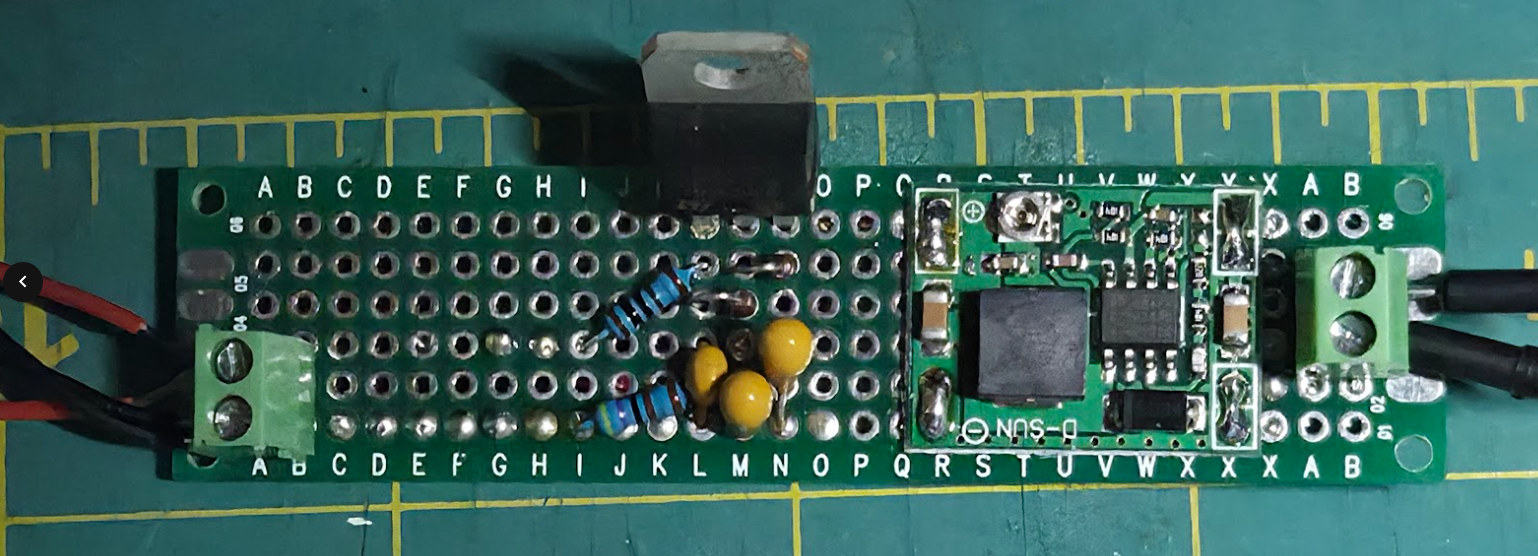
Power Section
So far the prototypes have been running from my bench power supply, but I wanted a bit more flexibility on the power source, allowing the board to run from a standard 12v wall adapter to be a bit more efficient on longer runs.
Each of the sections has their own 5v LDO voltage regulator to avoid coupling noise between the digital and analogue components. This presents two challenges:
avoiding adding noise from using a cheap wall wart
dropping 12v to ~7v to supply the voltage regulators
Whilst the boards use a tiny amount of power and the heat would probably be manageable, it seemed unwise to feed a potentially noisy 12v straight to the LDOs
The power section uses a small buck converter to initially drop from 12v (or more) down to ~9v. This is then followed by an LM317 adjustable regulator to clean the input and drop the voltage again to 7v. The LM317 provides the analogue and digital sections with a relatively clean 7v which is then tidied up again by the section LDOs.
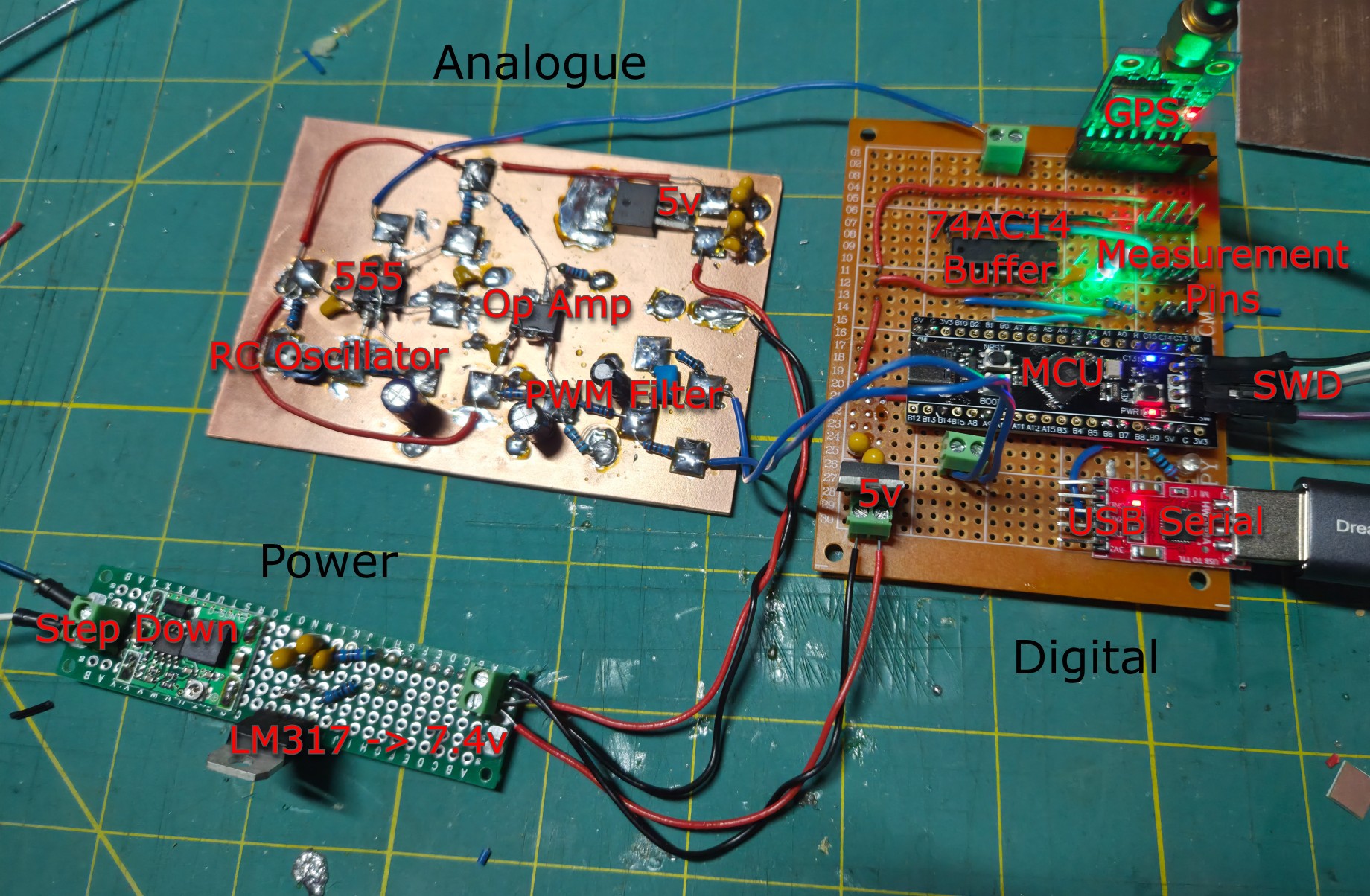
The Big View
Here's an annotated view of the final configuration
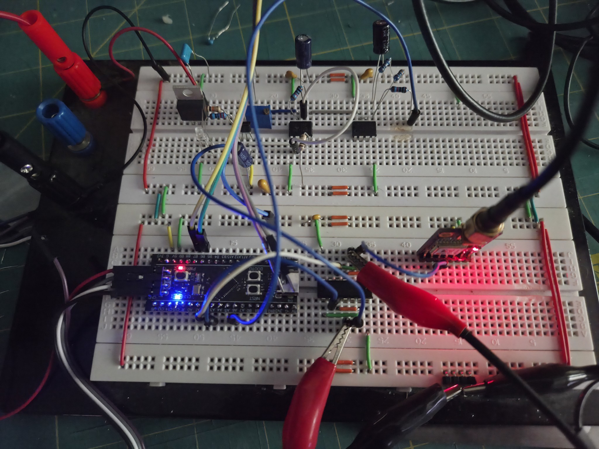
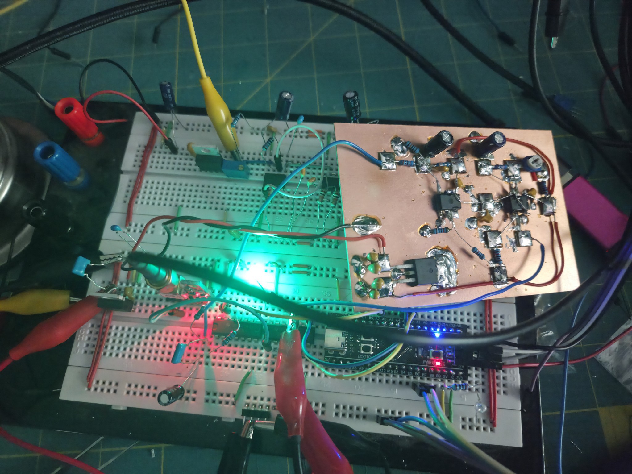
After seeing noise related problems in the breadboard prototype it's time to get a bit more serious about the build and break out the soldering iron.
The right answer here would probably be to design out a PCB with SMD components and get one of the Chinese fabs to build and ship it. But I'm impatient and I think this breaks constraint (3); a custom PCB is not something I have to hand and it's not cheap and cheerful.
The lowest noise way I know to construct circuits is a deadbug / manhattan style build so that's where we are going. It will look like a pile of junk but will hopefully be enough to get the noise floor down to somewhere 'reasonable'.
Refining the PWM FIlter
Part way through the build, testing out the PWM filter and with the old breadboard prototype still in situ.
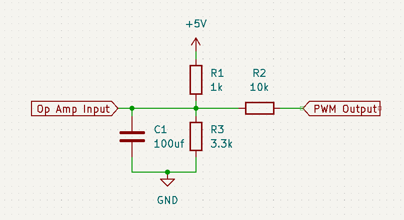
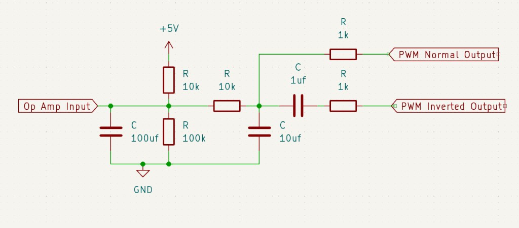
A key objective for the build is to improve the PWM filter and prevent leakage of the PWM signal through to the control voltage. The filter must effectively squash the 1.4khz PWM signal (moooaaar filtering) whilst also remaining responsive to control changes so that the PID functions (but not too much filtering).
Handily, stm32 MCU have an 'Advanced Timer' peripheral that can generate complementary PWM outputs. These can be used as described in the 'Active ripple suppression' section (page 4) to create a first stage filter with the addition of just a few more passive components.
The PWM filter now looks like this
In this configuration the filter is able to move the control voltage between 3.84v and 4.48v with approximately 9uV resolution.
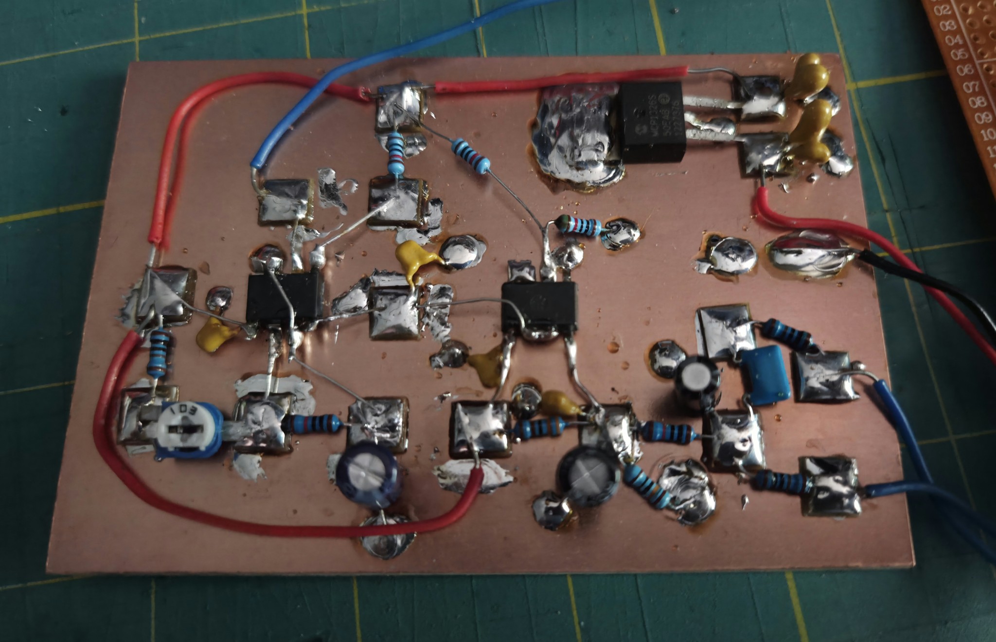
Final Board
Here's the built board in all its janky goodness, complete with excessive amount of bypass filters and solder.
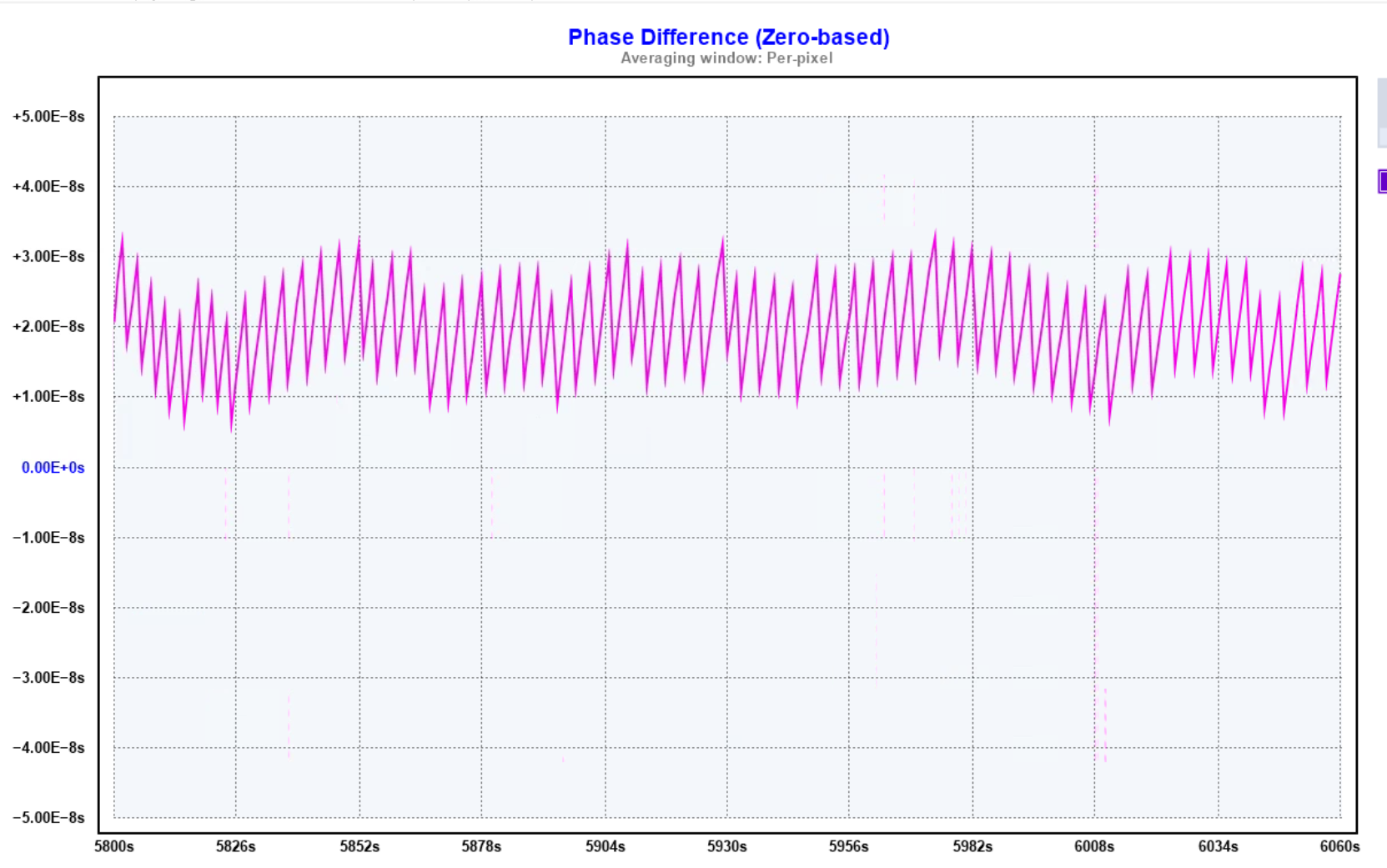
There is a persistent frequency offset and the PID is unable to zero the frequency difference
The frequency is way too flat and doesn't show any of the expected noise, there are also strange phase jumps where the frequency should be smoothly varying
There could be at least three possible causes for the errors:
a measurement error
a software problem preventing the PID from operating correctly
The TICC is a timestamping counter with a very high resolution (~60 picoseconds) and very low noise floor around 1e-10); it's designed to perform long running measurements of low frequency (PPS like) signals so is ideally suited to measure the 1hz output from the 555.
Using the TICC to graph GPS sawtooth errors:
The TICC requires a 10mhz reference clock and has two timestamping channels. By using a GPSDO reference and providing the GPS PPS and 555 PPS on each channel a three cornered hat measurement can be performed to compare noise across the three sources.
The TICC, GPSDO and a standard GPS PPS all have much greater stability than the 555 RC oscilltor by some margin (~4 or 5 decades, at least) so there should be good confidence that the 555 measurements are accurate and the problems seen do not lie here.
Software or Hardware Problem ?
To try and rule out problems with the PID software a simple test was created to sweep the PWM control voltage over a small range between 32768 (the centre frequency) and 33768 . The idea is to check the PWM is being generated correctly and the 555 is responding to the control voltage changes as expected.
Ooops, that's not right, not at all.
Two separate problems become apparent:
During the test the 555 PPS became roughly phase aligned with the PPS from the GPS signal and became injection locked. For a small period both signals are locked in sync and beat together exactly
Rather than smoothly varying with control voltage, the 555 frequency is being quantized in to step changes
Checking how far apart the quantization steps are reveals the culprit; each step is a difference of ~6E-4 which looks suspiciously like 65536 / 100,000,000. The smoking gun is pointing firmly at the use of PWM.
No Surprises
The control voltage for the 555 is very sensitive, with the each step of the PWM corresponding to just 3uV; any slight noise leaking through to the control voltage is going to influence the system.
Conversely, a plug in breadboard is not a low noise environment and creating the prototype with digital components sat together with the sensitive analogue components is asking for trouble. It was inevitable that the prototype would get problems somewhere, so it was interesting to see where this would manifest.
Next Steps
To improve the results we'll need a lower noise build:
The analogue and digital parts of the system need to be kept apart. Physically, with separate builds and electrically by separating the ground and power networks as much as is possible
The analogue portion needs to use low noise build techniques with a solid ground plane, no more breadboarding
The PWM filter needs beefing up to prevent the PWM signal leaking through to the control voltage
Bypass capacitors, _everywhere_
Spoiler Alert from the Future
Here's what a PWM sweep looks like in the final build.
The difference is clear, showing the 555 frequency smoothly varying with control voltage and that the PWM control steps are smaller than the inherent noise of the 555 RC oscillator.
Another Spoiler Alert from the Further Future
A typical GPSDO will incorporate sawtooth correction to improve accuracy and reduce averaging times. This is not going to be required for the 555 as it performs way worse than the GPS PPS, even without taking sawtooth in to account.
The second prototype makes a number of improvements over the first
The stm32f103 (Blue Pill) is swapped to an stm32f411 (Black Pill). The stm32f411 has a 32-bit timer allowing it to count a full 1 second period of 100 million ticks without overflow. This considerably simplifies the timer code and avoids potential race conditions that can occur with a 16bit timer and dealing with overflow.
Power is now provided by a 5v LDO regulator driven from my bench power supply rather than the USB socket of the microcontroller. The flipside to now having plenty of spare power is that I can no longer use the USB serial on the microcontroller and have to add a serial to USB converter and output debug via the USART. The blue/black pill designs do not isolate the USB socket so you are unable to have both the USB and an external 5v supply connected.
A 74AC14 Hex Schmitt trigger has been added to buffer the PPS from the 555 and GPS receiver. The 74AC14 allows adding led's and measurement probs without overloading either of the sources.
With the initial prototype, it became clear that additional PWM resolution would be required so the PWM filter was tightened a bit
The PWM control voltage is now roughly 3.64v to 3.84v with a resolution of 3uV per PWM step.
The first prototype software had 16bits of resolution when comparing the 555 and GPS frequencies. This was also increased to 24bits. This should be way overkill, but I've paid for all those bits and I'm going to use them.
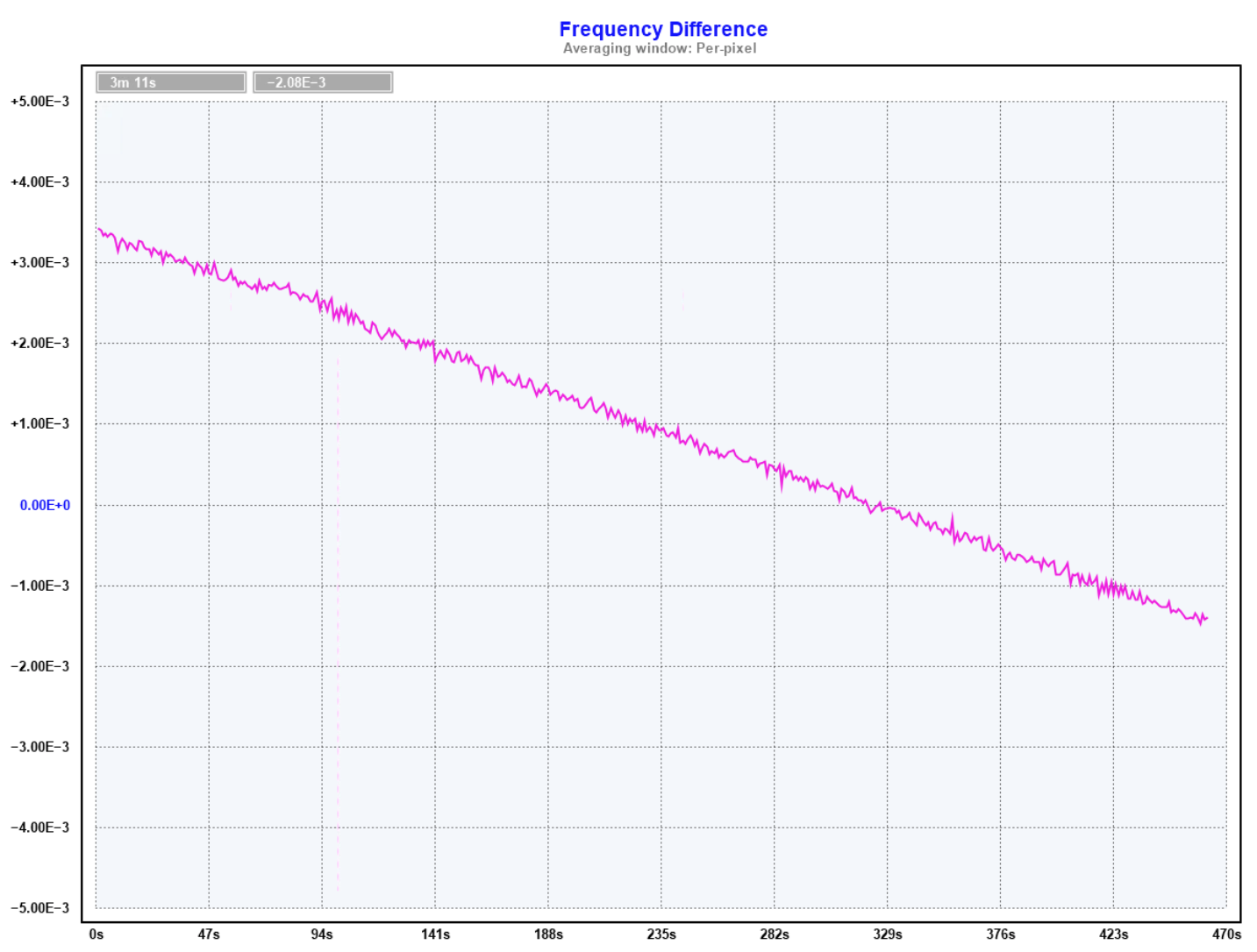
The result is good
But actually that is _too_ good.
The spikes in frequency also indicate that the phase is being stepped rather than smoothly varying.
Zooming in shows a persistent 2.75e-5hz offset in frequency
Both the stepping and frequency offset can be clearly seen in the phase difference
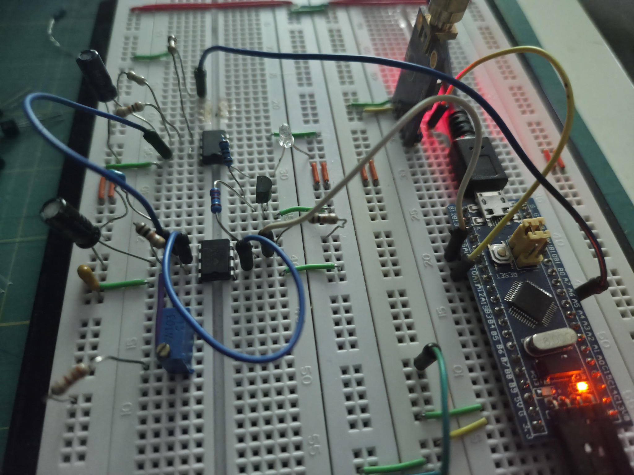
The first step in the project was to quickly get a prototype running to test the concept and get an initial idea on where some of the challenges may lie
PWM Filtering
The MCU runs at 3.3v and uses a 16bit timer for the PWM signal, therefore providing 65k levels over a 3.3v range. The 555 however is operating at 5v and a full 3.3v range is way too much, so a simple PWM filter was chosen to shift up the PWM voltage and narrow the range:
The filter provides a lower bound of the PWM at ~2.24v and an upper bound at ~3.5v with a resolution of around 19uV per PWM step.
Success !
The prototype was able to demonstrate management of the 555 frequency using the control pin and a basic PID was able to bring the frequency to 1 hz:
Approximately anyway, it's pretty noisy and we should be able to do better.
The first problem also became apparent pretty quickly ...
Powering the prototype via the microcontroller USB connection wasn't going to be enough and a separate power supply with regulated voltage was going to be required.
 burble


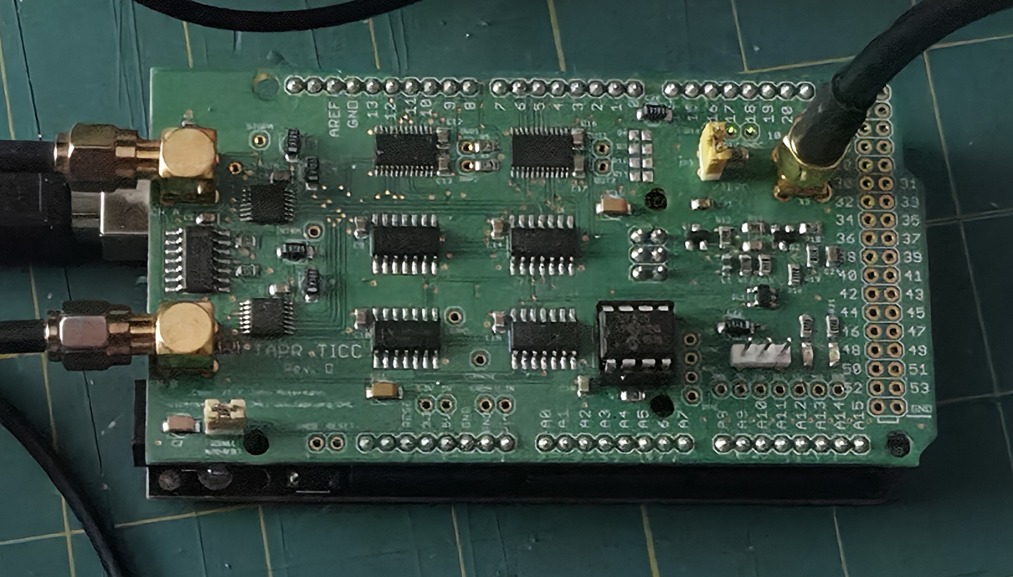
 The TICC requires a 10mhz reference clock and has two timestamping channels. By using a GPSDO reference and providing the GPS PPS and 555 PPS on each channel a three cornered hat measurement can be performed to compare noise across the three sources.
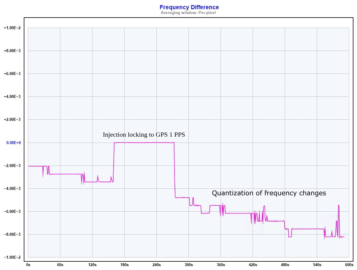
 Another Spoiler Alert from the Further Future