Yann Guidon / YGDES
-
YGMII7-16
04/11/2026 at 19:58 • 0 commentsLet's start with an easy implementation, with the simplest protocol:
- 4 bits in parallel
- 1 bit of bus inversion
- 2 bits of clock (QA, QB)
- 16 bits per word (suitable for mono sound @16 bits or stereo @8bits, or for AI floats, or whatever)
- Easily extended to 32 bits in "OctoDataRate" (ODR) instead of QDR.
As usual, the data precedes the clock transition so the emitting circuit is DDR, running at 1 clock cycle per nibble. So it's "simple, synchronous design" and should not be hard to design.
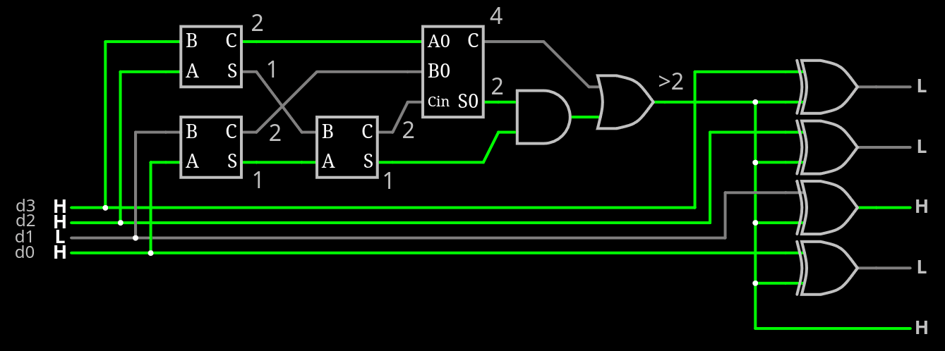
So let's start with MAJ4 to toggle the bus. That makes 5 bits and 6 counts:
- 0, 1, 2 : BI=0
- 3, 4 : BI=1
The circuit here is a reduced version of the previous ones.
![]()
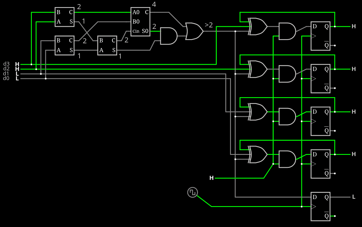
Adding the buffer is pretty simple, as shown in this extended circuit:
![]()
Just be sure that it's possible to synchronously clear the output.
So foor, so gad.
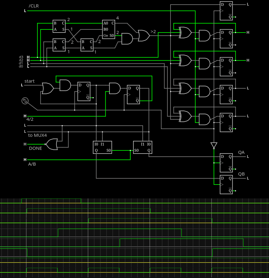
Then it becomes a bit more funky, as the clock generator must be designed. It's based around the classic "quadrature counter" or "2-bit Johnson counter" or "2-bit Gray counter": that's all the same circuit. It must generate at least 4 sequences:
- 4 cycles 2 3 1 0 : data A
- 4 cycles 1 3 2 0 : data B
- 2 cycles : 1 0
- 2 cycles : 2 0
One half can be realised by swapping the outputs with a pair of MUX.
The other half controls how signals are generated and circulate between the registers.
![]()
- A/B selects the order/direction.
- START is a one-cycle long pulse that triggers the sequence
- DONE goes high when the sequence is finished (returned to state 0)
- The state is also brought outside to select the nibble using an external MUX4.
- Extension to 32 bits will toggle A/B, which also controls a 32->16 MUX2.
- 4/2 selects the length of the sequence, often used with /CLR to reset the state.
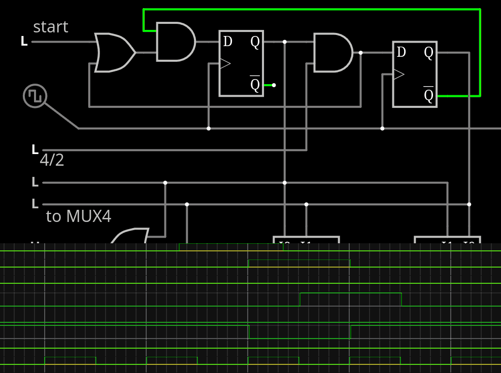
OK I made a tiny mistake for the one-shot sequence, the feedback is behind the AND2:
![]()
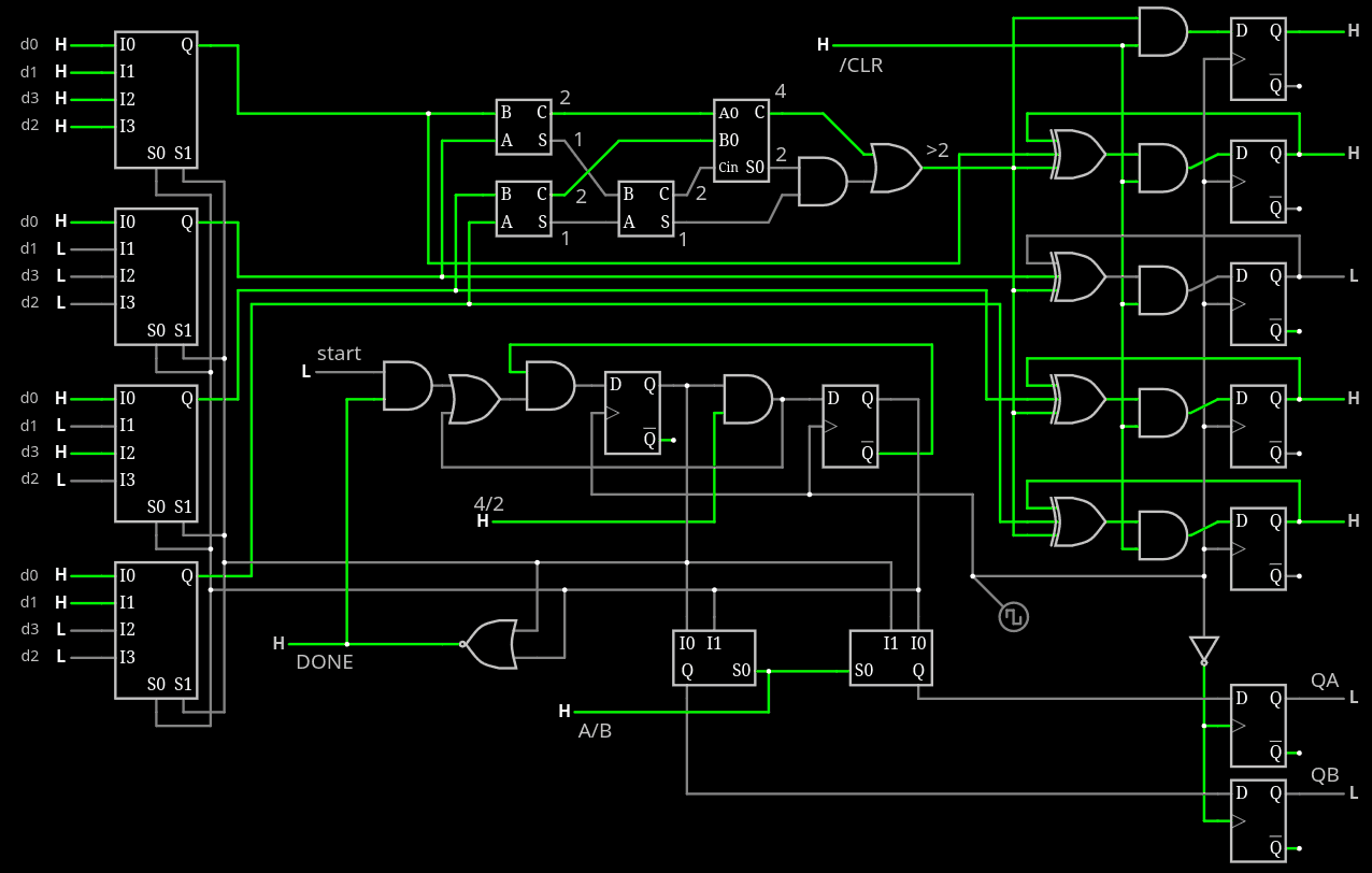
So all that's left for a transmitter is the 16->4 MUX4, which is quite large/cumbersome with CircuitJS but you get the idea. As you can see:
![]()
I have added a protection to the START signal so it can only work when DONE.
And then, one still has to design the FSM, but you see it's not difficult with the control and status signals:
- START
- A/B
- 4/2
- /CLR
- DONE
The decoder/receiver is a different pizza party though. This is why I create the "easy" encoder, so I can get the decoder right.
-
16-bit mode
04/02/2026 at 19:15 • 0 commentsA number of other applications work with 16-bit words, they don't seem to need control and/or parity.
From there it becomes easy to use the saved 2 bits as TMPI/inversion bits, using one bit for the inversion and 4 bits of data/payload.
Going 32-bit is as easy as : one 16-bit word (4 cycles) with one clock direction, and another word is the opposite clock direction. An "aborted" cycle would do the framing.
At that point, I wonder if/how the clock signals could become part of the inverted word, and how to recover the combined transition/word (3 down to 2 signals), if it's even possible... => the answer is "it does not matter":
- 4 data bits get TMPI => 5 bits where only 3 change
- 2 clock bits where only one changes
- total : 4 bits change over 7.
If the clock signals are TMPIed, then that's 6+1 bits => 4 changes.
Result/change is the same, but one is simpler and more straight-forward, following the existing clocking scheme.
-
Transition density
03/29/2026 at 20:47 • 0 commentsHere is a First sim:
![]()
The popcount is applied over 9 bits so it's not possible to prevent simultaneous switching of all 5 wires. But the overall density of transition is clearly decreased: there can not be more than 5 transitions during 2 cycles. Over a longer transaction, this keeps the general EMI spectrum more stable.
That's all can be afforded with only one half of a bit for Transition Reduction, one can't talk about Transition Minimisation at this level, but at least it's something. And it's nice to share the XORs between two bits.
-
Pin layout
03/29/2026 at 19:33 • 0 commentsThe 7 wires should be organised and ordered to reduce EMI and crosstalk.
I expect the wires to lie in parallel on a PCB, usually over a ground plane and/or interleaved with parallel ground traces
D0 g D1 D2 g D3 D4 g A B
- D0 is at the exterior and is likely to be "most active" as it would transmit the often-changing Inversion bit. But the inversion operates on a 10-bit pair so it gets paired with a half-changing bit.
- Clock signals A and B are usually transitioning 2× per 4-cycle data transaction, so it's almost guaranteed that only one transition per data transaction occurs, reducing the need for immediate grounding. Of course more grounding or pairing is good, but we're talking about minimal requirements here and the clock wires are somehow shielded from the two neighbour data wires D3 / D4.
Pins can be renumbered, such as
A B g D0 D1 g D2 D3 g D4
and the inversion bit would be D4. But this shows the influence of data transition statistics over the circuit's geometry, and one data bit is not "like the others" and would be placed apart.
-
Data latching
03/29/2026 at 13:37 • 0 commentsSending/generating any type of data is trivial. Receiving is hard, and the higher the frequency, the harder it gets.
In the case of YGMII, data are "source clocked" which means the stream is more or less asynchronous to the receiver. A proper FIFO is required but that's not the real problem. Missing a word that arrives too late for the PHY ? => insert an IDLE symbol and that's it.
Now getting the clock is something else and it's asynchronous. Adding a PLL will only increase the problems of jitter (on a wire or system-wise). And then you have to demux and process the FSM.
One thing helps though : there are an even number of edges on each clock wire A and B to complete a transaction. So each transaction is made of at least 2×5 bits. The data transaction with 20 bits is one case among others, even the CLEAR or STATUS transactions need 2 cycles and carry 10 bits of payload.
This means that for each clock signal there is a pair of edge-triggers D latches, each triggered by a different edge polarity. And the FSM can be built from this distributed collection of four rows of DFFs.
.
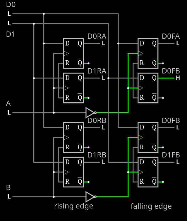
The following example shows only 2 of the 5 bits for clarity, and illustrates the fundamental idea/principle:
![]()
This system is inherently asynchronous and in the end requires resynchronisation with the host/receiver, but this can be done with a handshake on larger words, at a slower frequency. This flexibility enables faster transmission rates and some small amount of jitter between the emitter's clock and the receiver's.
.
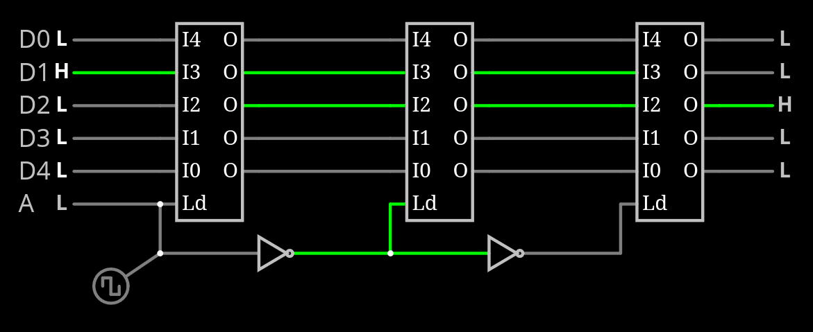
Note that each DFF is a pair of transparent latches, so 2 DFF clocked by opposite fronts could be merged. This leads to a "triple latch" structure to reduce redundancy and footprint:
![]()
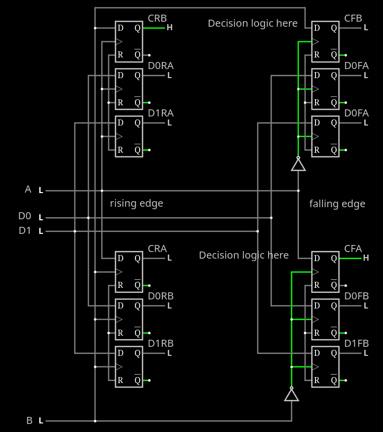
But this optimisation will come later. And it's only the beginning because the clock-controlled FSM should run in real time, updated at each incoming front. This leads to a "distributed FSM" where each of the 4 zones is activated in turn, and updates its state by reading the other's clock signal value and the other states.
Extending the binary decision tree from the last log, we add the criterion of parity and we find that the FSM can return to the "IDLE"/End of transaction on the falling edges, so every other row of decision.
- CLEAR and STATUS can be reached after 2 transitions, of the same signal, with the other never moving.
- DATA and CONTROL are reached after 4 transitions
This means that the FSM logic can be concentrated at the inputs of the falling edge registers.
And when the transaction is complete, the temporary status stored in the rising edge registers is cleared. Or something similar. So a new transaction can be decoded again.
The result:
![]()
Each rising edge layer registers the state of the opposite clock, and from there the falling edge can determine which type of transaction ends.
-
Clocking
03/29/2026 at 02:51 • 0 commentsThe interface uses 2 clock signals: this provides a reasonable EMI reduction and it also extend the protocol.
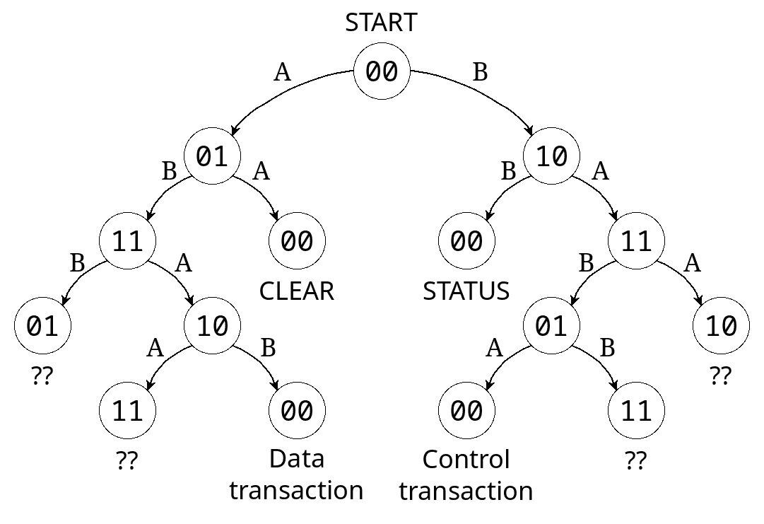
The 2 clock wires are required to encode the 4 edges of a full transaction in normal/usual mode. The signals follows the traditional Gray counting sequence:
00
01
11
10
and the whole transaction is ended when both signals are back to 0.
Swapping the sigals corresponds to counting in reverse:
00
10
11
01
This signals that the transaction contains a control or status word.
There is a rule that only one wire can change at a time and each front updates the state of a sort of FSM.
Naming the clock signals A and B, we get a sequence of these letters and the sequence ends when the number of As and Bs are both even.
Thus we get these 4 basic sequences:
AA : reset AC register  (set to current value ?)
BB : Update link status (9 bits?)
ABAB : Data transaction (18 bits)
BABA : Control transaction
Another way to visualise is with a binary decision tree:
![]()
You get the idea: the protocol is extensible and we start with a few good cases that are easy to use without too much complexity.
YGMII
YG's Media Independent Interface, in case your miniMAC is on a different chip than your miniPHY