Yann Guidon / YGDES
-
Synthesis checks
08/07/2020 at 22:09 • 0 commentsI tried to run my new code through Synplify (in the Libero SOC suite) and got some interesting results.
First :
I finally understand how to create and use external libraries, in particular the SLV lib worked right out of the box, after I searched for the right method. It's some of those dumb painful GUI clickodrome that looks nice during a presentation but is not possible to automate... Anyway, SLV_utils.vhdl was added smoothly.
Second :
I forgot an important "detail" about how Synplify wants its external entities : "old style"... So I had to adapt/modify a lot of lines. Nothing changed except the syntax. It's more verbose, you have to add a declaration for each block you use... But now it works.
Third :
I could check, verify and compare the behaviour of the synthesiser with various versions of one unit.
In particular I verified that the "balanced control tree" approach is beneficial compared to the dumb/usual approach. Log 25. MUX trees gets a graphical update :-)
Oh and I found how to manually place & lock gates, so here is one test with INC8 :-)
![]()
The system was not able to optimise this unit more so I guess I'm not far from a great design.
Now, I just have to find how to generate these coordinates with a program and send them to the tool...
Finally :
All the modified and/or tested VHDL files have been re-integrated into the code tree with the following line :
-- SYNTHESIS OK
So it's easy to check/list all the final files with grep, and separate them from the simulation-only files :-)
I have gained more insight, refreshed my skills and proved that my method works.
-
TAP v.2
08/04/2020 at 22:20 • 0 commentsAs I am near completion the design of the TAP system, I realise I have harder and harder timing problems to solve... And I could even save some gates !
The Counter has 32 gates. The Gray counter has 17. Both count on CLK's rising edge and mayyyybe... they could be merged ?
It's not difficult to adapt the Gray counter to provide the additional signals FB (Full Byte : just a NOR3) and SAT (an added DFF and a couple of gates), as well as individual decoded size output signals for 1 to 8 bytes (though so far only 2 and 4 are used). Overall, the Gray counter would expand to maybe 30 gates, which would overall save maybe 20 gates compared to the split design, and the DFF would not have a RESET input, which might be absent in ASIC gates libraries (and use more silicon)...
The harder part though is the transition between the 2 phases and the reset of the counters. I think I have an idea but it will force me to deconstruct the Gray counter into a more traditional logic+DFF system, because... it will become a classic digital sequential circuit, with the current state and the expected new value that may (or may not) be latched.
20200808 :
Some more thoughts gave this result :
![]()
This easily solves the question of using the counter with BOTH phases, at the cost of 1×DFF, 1×XNOR and 1×AND2 per counter DFF.
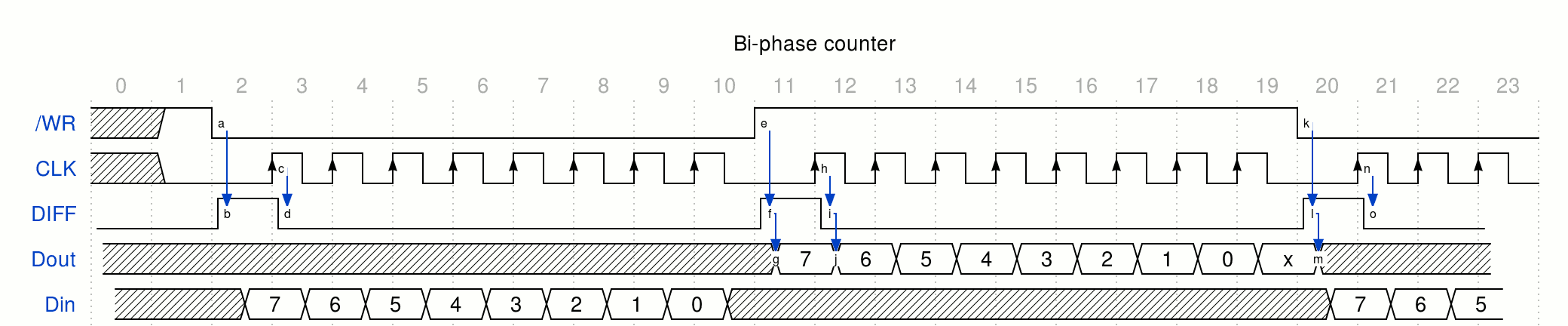
Here is how it shoul look with wavedrom :
![]()
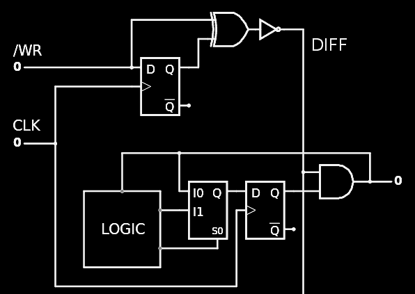
This does not solve however the case where /WR is toggled up and down without CLK activity. The DIFF internal signal should be "sticky" and go back down when CLK has a rising edge...
There, it should work now :-) (ok it doesn't because of a race condition with the clock)
![]()
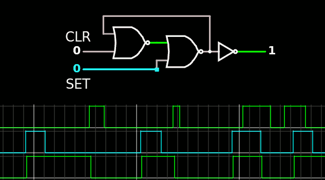
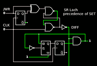
Each time /WR changes, the added DFF is RESET, and later set again by a positive edge on CLK. The question now is how to emulate this DFF with individual gates. The following circuit seems to work well and is adapted to ASIC implementation :
![]()
The two NOR2 use little surface on a die. The output inverter works as a buffer. There is no oscillation condition, as proved in the above trace : the SET has precedence over CLR, which avoids the race condition found with the initial idea using a DFF. The initial value of the latch is determined by toggling the /WR and CLK pins and a short initialisation sequence brings the circuit to a know state:
- bring /WR low
- pulse CLK once (at least, could be more) => first DFF state is known
- set /WR high => changes XOR => CLR the SR latch
- pulse CLK once (at least, could be more) => SET the SR latch
The output data can be ignored, shift 0s in to make NOPs (just in case). So this could be summed up as : shift a NUL byte in, then shift a dummy byte out.
Here is the new version :![]()
Note : this works ideally when the CLK input is LOW when /WR changes. However : to create a rising edge, CLK must go down before going up again, this half-clock phase (when low) will be the "clear state". Ensure this period is long enough and that the CLK state is appropriate (check on the 'scope to be sure !!! I'm looking at you, Raspberry Pi...). This is not critical while shifting bits in, however it is a delicate thing to ensure when reading from the TAP (in particular, the first "volatile bit").
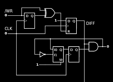
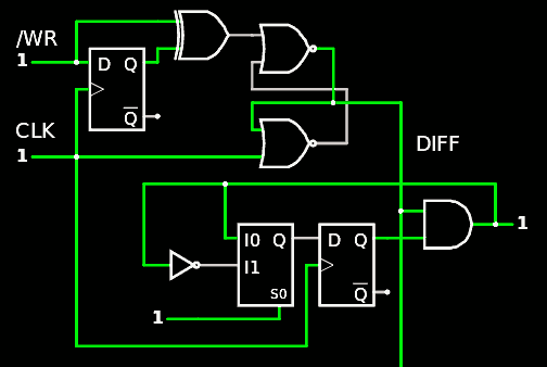
This is solved by changing the precedence of the RS latch to RESET/DIFF/WR, as in this updated circuit :
![]()
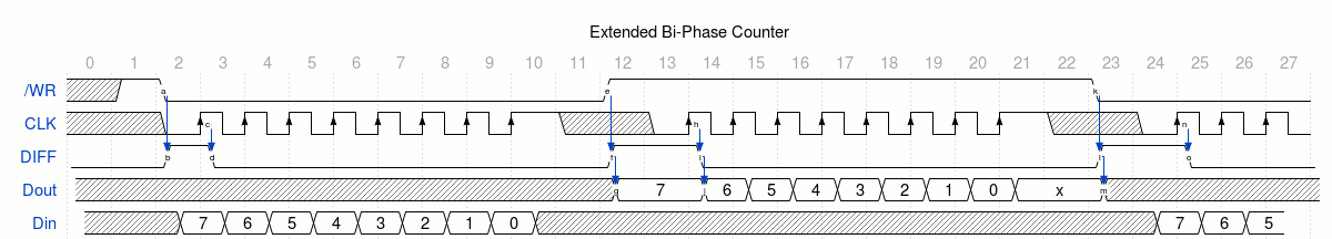
And the extended chronogram :
![]()
Now CLK can go low before or after /WR changes.
Just by changing where a wire is connected.
-
The TAP crosses 3 clock domains !
08/03/2020 at 17:52 • 0 commentsThe eXecute module of the TAP connects one domain with no RESET but 2 clocks, to another with one RESET and one clock. This makes it more complex than the others, as hinted by the end of the previous log The TAP's eXecute module.
- On the TAP side : CLK and /WR are two sources of clocking. CLK goes to the counter and the shift registers, /WR goes to the decode logic that takes the control at the end of each message.
CLK would not go very fast : 10MHz is reasonable (wires and other external effects would probably disturb the signal) and leaves 100ns between consecutive rising clock edges.
There MUST be a reasonable margin (100ns ?) between the last rising clock edge and the rising edge of /WR.
There is no RESET for several reasons :- The TAP must be able to work while the rest is in /RESET
- Adding a TAP-specific RESET pin would increase the external footprint and wiring
- The TAP can control /RESET from the inside
- Routing another /RESET could burden the rest of the chip
- By design, the TAP will work with the proper init sequence. (JTAG can also work without /RESET pin)
- The core has a free-running clock, as well as a HW /RESET external signal.
The clock could be as slow or fast as one wants, or even weird...
The /RESET can also be overtaken by the TAP.
.
.
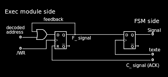
For the communication with the FSM, the signal goes through two DFF as shown below :
![]()
If the FSM clock is fast enough, the OR can be removed but... you're never too sure ! For example going from RESET to START triggers the reload of the instruction memory, which can take 4K cycles at least.
The first DFF triggers on /WR going up, which is the necessary condition to detect the end of the message, or else the "valid" address could be trigered by enough random data flowing through the shift register. The asynchronous RESET allows the crossing of clock domains, and the clearing always trails the setting by at least one FSM clock cycle, as delayed by the next DFF.
The DFF on the right also re-synchronises the input data so it is valid at the start of each FSM clock cycle. Otherwise the data could arrive late in the cycle and create race conditions and invalid boolean calculations.
.
.
- On the TAP side : CLK and /WR are two sources of clocking. CLK goes to the counter and the shift registers, /WR goes to the decode logic that takes the control at the end of each message.
-
The TAP's eXecute module
08/01/2020 at 12:43 • 0 commentsThe previous modules are quite simple, easy, self-contained, while the X command (described earlier) subtly touches more things at once.
![]()
Talking to the Instruction slice is not very hard, but requires some decoding first, and some of it would be best shared with the Selector. The "addresses" 'S' and 'X' are very close and and this would save some gates.
I think it's the perfect time to talk about how I mapped the S-decoder to gates :-)
It started easy enough for the 'S' condition :
valid <= '1' when  SRi( 7 downto 0)="01010011" -- signature
        and SRi(15 downto 11)="00110"   -- command : MSB select ASCII chars '0'-'7'
        and SAT='0' and W='0' and J1='1' and J0='0' --    else '0';
Then another simple step is to sort the '0' and '1' to put them in two separate equations, one with AND for the '1's and the '0's are gathered with a big NOR :
norx <= not (SAT or W or J0 or SRi(15) or SRi(14) or SRi(11)
             or SRi(7)  or SRi(5)  or SRi(3)  or SRi(2));
valid <=  SRi(13) and SRi(12) and SRi(6) and SRi(4)
              and SRi(1) and SRi(0) and J1 and norx;
Then it's easy to group the ORs and ANDs together into 3-inputs gates. And when there are not enough inputs for the AND gates, they can be used to input the result of the NORs :-)
Finally, bubble-pushing can transform two consecutive ANDs into a NAND followed by a NOR.
So let's do this all over again but this time the X condition is also decoded so some gates are common.
S <= '1' when SRi(7 downto 0)="01010011" and SRi(15 downto 11)="00110"
                    and SAT='0' and W='0' and J1='1' and J0='0'
   else '0';
X <= '1' when SRi(7 downto 0)="01011000"
                    and SAT='0' and W='0' and J2='1' and J1='0'
   else '0';
The common terms are
COM <= '1' when SRi(7 downto 4)="0101" and SRi(2)='0' and SAT='0' and W='0'
  else '0';
and S and X can be taken separatey :
S <= '1' when SRi(3)='0' and SRi(1 downto 0)="11" and SRi(15 downto 11)="00110"
                    and J1='1' and J0='0'
   else '0';
X <= '1' when SRi(3)='1' and SRi(1 downto 0)="00" and J2='1' and J1='0'
   else '0';
Now these 3 can be checked in parallel, let's separate their bits according to their value.
X <= SRi(3) and J2 and
       not ( SRi(1) or SRi(0) or J1); -- nice fit for this one !
S <= SRi(1) and SRi(0) and SRi(13) and SRi(12) and J1 and
       not (SRi(3) or J0 or SRi(15) or SRi(14) or SRi(11));
COM <= SRi(6) and SRi(4) and
       not (SAT or W or SRi(2) or SRi(7) or SRi(5));
From there the gates are easy to cluster and bubble-push.
The result is 11 gates, the speed is not striking but 4 or 5 gates of latency shouldn't be limiting for this slow circuit and it is only 2 more gates than the previous circuit.
   sa: entity  OR3 port map(A=>SRi(15), B=>SRi(14), C=>SRi(11), Y=>tSo  );
   sb: entity NOR3 port map(A=>J1     , B=>SRi( 3), C=>tSo    , Y=>tSn  );
   sc: entity AND3 port map(A=>SRi(13), B=>SRi(12), C=>tSn    , Y=>S2   );
   sd: entity AND3 port map(A=>SRi( 1), B=>SRi( 0), C=>J0     , Y=>S1   );

   c1: entity  OR3 port map(A=>SRi(2) , B=>SRi( 7), C=>SRi( 5), Y=>Co1  );
   c2: entity NOR3 port map(A=>SAT    , B=>W      , C=>Co1    , Y=>Co2  );
   co: entity AND3 port map(A=>SRi(6) , B=>SRi( 4), C=>Co2    , Y=>COM  );

   x1: entity NOR3 port map(A=>SRi(1) , B=>SRi( 0), C=>J2     , Y=>tXo  );
   x2: entity AND3 port map(A=>tXo    , B=>SRi( 3), C=>J1     , Y=>tX   );

  vx:  entity AND3 port map(A=>tX     , B=>COM    , C=>FB     , Y=>X    );
  vld: entity AND3 port map(A=>S1     , B=>COM    , C=>S2     , Y=>valid);
(one thing I dislike about VHDL is the requirement to label ALL the instantiated entities, it really gets nasty fast).
OK !
- Now, the Selector decodes the execute address with only 2 gates of overhead.
- The clock to the slice is only gated by /WR, already done by the Selector.
- The data to the slice shift register comes directly from the Selector as well (the MSB of the Command bus)
But the slice requires more than these signals and the FSM is an even tougher beast... Let's just focus on the control of the slice :
- Imux : the source of the instruction is selected by the current command (STEPX, NOPX ?) which requires some decoding.
- TrapEn : only active with the START instruction with Trap flag active. This will need extra care to prevent weird conditions when more units are added !!! For now it's only gated by /WR.
- MaskEn : only active with the WrMask command, gated by /WR. as well (beware of timing and levels).
- And there are the START/STEP/STOP/RESET signals to send to the FSM...
But this is getting hard because these signals cross clock domain boundaries.
On top of that, I can't use the other timing tricks because one can't ensure the length of the binary stream (since it's always shifted, no gating) and I can't use a latch because /WR must be the clock => a transparent latch would output a strobe/signal before the end of the message, which could be longer and be an invalid/spurious signal...
For most of the signals, I have chosen to use a DFF, some are simple (output the result of the decoding logic), others (the FSM strobes) are "set" by the decoding logic, then the FSM itself will send an ACK/Clear signal that will asynchronously reset the signal. The DFF's output will then be resynchronised by another DFF inside the FSM.
And then, you need to reset these DFF because they are in unknown state on power-up : one of the Selector addresses could be used for this.
But two other signals create really big timing problems.
- Mask latch : this is a strobe, needs a DFF, but the DFF will keep the value even after the /WR strobe is back to 0. A AND must be added to the output, or maybe /WR could be tied to a /RESET input ? (the timing and logic would be very dirty and unreliabe/unportable)
- the Write Instr Mem command depends on an externally clocked SRAM array so a handshake is required too...
continued in The TAP crosses 3 clock domains !with some diagrams...
-
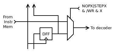
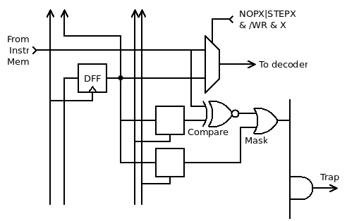
Trap on instruction
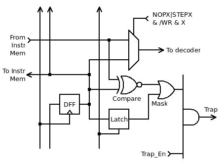
07/30/2020 at 06:15 • 0 commentsFrom the very beginning, the Y8 core is designed to allow extensive debugging features. Look at the early logs 3. Breakpoints ! and 4. The YGREC debug system to see the approach.
As the TAP system is being defined and implemented, more details emerge and here I describe one sub-sub-part of the debug system : the slice inserted between the instruction memory and the instruction decoder.
![]()
This DFF+MUX2 is pretty easy to design & layout, and the insertion delay is short enough, so why not add more features ?
The early drafts promised a trap on a given instruction. This can be refined by masking some of the bits to compare and we get two registers (CoMPare and Match). Since latches uses 1/2 the size of DFF and we have a DFF very close, 2 latches are chosen.
![]()
This is very helpful during debugging because you don't have to focus on a particular instruction.
- Want to know how many times a given opcode is executed ?
- Want to know which instructions write to a give register ?
- Want to know why a given I/O register or range is overwritten ?
Just set the mask to select the desired field (opcode, register, immediate...) and select the behaviour (trap or count) and you're done.
Some more considerations and compromises...
![]()
I dumped one latch to save space. That's the difference between 80 and 96 gates, in a core that is already quite small.
This means that the mask latch must be loaded first then another command loads the instruction chain again, and can't change it at all, so a specific command must also assert Trap_en only when /WR is high while sending a "START" command to the FSM.
The control logic is slightly more complex but the compactness matters. Fewer gates means fewer sources of errors, delay or power sinks.
Just added YGREC8_VHDL.20200730.tgz that includes the TAP/Slice circuit shown above.
-
TAP summary & protocol
07/29/2020 at 15:34 • 1 commentFirst, here are the logs that describe the design of the Test Access Port :
4. The YGREC debug system contains the first high-level description, the principle applies equally for any technology/implementation.
16. Inspect and control the core
24. Synchronous Serial Debugging
25. MUX trees
109. Gray counter (reboot of the low-level design)
110. The art of large MUXes
111. The first half of the TAP
112. Design of a TAP : the SIPO Controller
113. The TAP's bits counter
114. The TAP selector
115. The TAP is coming together
118. The TAP's eXecute module
119. The TAP crosses 3 clock domains !
.
This log summarises the high-level view from the debugger's perspective. The TAP is "just" a low-level port, a few pins that serialise data in and out of the core, and could be implemented in whatever way (the current TAP is serial but could be made in byte-parallel for the relay version for example).
This TAP is obviously byte-oriented and designed for SPI mode 0 : this eases programming a lot because most CPUs have a byte-oriented SPI controller. Using variable sized framing would operate slower on platforms such as the Raspberry Pi for example. JTAG often handles sequences of bits in groups other than 8...
Timing
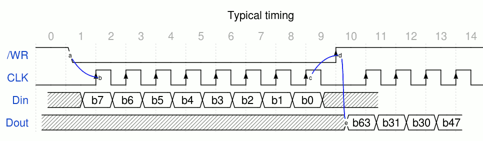
The diagram below shows the typical timing with only one transmitted byte shown:
![]()
The TAP works as 2 phases in half-duplex, so Din and Dout may share a tristate pin for example. The /WR pin controls the phase and things happen during these transitions.
- Going from high to low starts transfer on Din into the TAP, "full bytes" at a time (the number of bits is always a multiple of 8, MSB first to follow the common SPI standard). Each bit is sampled on the rising edge of the clock. The delay from a to b , as well as c to d, is typically one clock cycle to give enough settling time to the internal counter.
- Going from low to high starts the shifting out of the data from the TAP to the host controller. The 64 bits are serialised with the MSB first, followed by bits from shuffled positions. Bit 63 is presented very soon after the transition (see d->e) so it can be polled without having to shift data or trigger a SPI byte shift. If more than 64 clock pulses are sent, the internal counter wraps around and serialises the same sequence of bits (though their values might have changed since).
The MUX
For practical reasons, the Y8 has a selection of 64 bits to provide a (partial but sufficient) snapshot of the core's state. Instead of reading all the registers, only 4 byte values are available (SND, SRI, Result & PC), which already amounts to 32 bits. The remaining bits are further halved by providing the current instruction (16 bits). The rest is shared by the Status Flags (C, S, Z : 3 bits), the FSM status and a free byte (possibly multiplexed with the scan chain for a loopback test).
In a sense, the order matters little because the bits are scrambled anyway. With the serial TAP, the user must stream 64 bits every time to get everything (this is not the case though for the scan chains and this saves some time). However it's "good" that they fit with the structure of the tree, so it helps with place&route. "Just in case" I placed the fields in increasing order of granularity and relevance to the debugger (in case a byte-wide, or non-scrambled, interface is developed).
TAP/MUX64 allocation of the inputs :
8 bits : Status (Flags & FSM)
8 bits : (undefined, variable, switchable, maybe the selector address ?)
16 bits : Current Instruction being decoded
8 bits : PC
8 bits : RES
8 bits : SRI
8 bits : SND
Notes:
- If a byte-parallel interface is defined, it gets the status immediately, without having to scan past the other bytes that might be unnecessary in a given context)
- This map is defined to be valid after a Null command, where the Selector is reset. Other registers (such as the breakpoints) could be selected by the Selector
- The debugger gets these 64 bits, regardless of the actual implementation : that is the "view" for the GUI which has to manage higher-level multiplexing, sequencing etc.
- The order of the bits matters. Beware with the mapping of MUX64 which can be bit-reversed or byte-reversed. The transient b7 of the first byte is always output first (even before the first clock pulse is sent) regardless of the permutation. This is used to poll the state of the FSM and check when a Trap occurred (for example). Instead of shifting all the 8 bytes, the controller can simply read the Dout bit repeatedly, without sending a clock cycle.
- To ease writing, the internal count order is reversed by the MUX64, so the Most Significant Bit always comes first. VHDL vectors are usually "downto" direction...
- Definition of the first byte :
Byte 1: Status (Flags & FSM) (MSB first)
    b7 : RUN state from System FSM (transient)
    b6 \ System FSM state
    b5 / (RESET, LOAD, STOP, STEP)
    b4 \ Instruction FSM state
    b3 / (IDLE, INST, LDCX, WrPC)
    b2 : Zero flag
    b1 : Sign flag
    b0 : Carry flag
The scan chains
The previous logs have already defined a number of messages :
- NULL : toggle the /WR pin without changing the clock line. This resets the Selector register and should get a clean state, like a RESET (which the TAP doesn't have).
toggle /WR high (just in case)
toggle /WR low
toggle /WR high
- Select : 2-bytes message
toggle /WR low
byte 1: chain selection (valid values : ASCII '1' to '6' so far, avoid '0' and '7')
byte 2: signature=ASCII 'S'
toggle /WR high
This enables one of the sub-chains. To select the chain 2, just inject "2S".
- Execute : This 4-bytes command is very powerful. It is always active, regardless of the selection. This means that the instruction word will be flushed every time new data is shifted in (but in most cases this is OK).
toggle /WR low
byte 1: Instruction MSB
byte 2: Instruction LSB
byte 3: Command
byte 4: signature=ASCII 'X'
toggle /WR high
The command byte must handle 2 things :- What to do with the 16 bits ? The instruction is stored near the decoder's input but should it be used/Muxed ?
- The command/message sent to the FSM. This is how you send the Start/Step/Stop/Reset commands (and others).
* bits 7, 6, 5 : reserved / not decoded
* bit 4..1 : FSM command
4321 : bit
0000 : NOP
0001 : STEP
0010 : START
0011 : STOP
0100 : RESET
0101 : Write TAP word to instruction memory at address PC.
0110 : Write TAP word to compare mask buffer
* bit 0 : Instruction MUX
    0 : Decoder reads instruction from the Instruction Memory
    1 : Decoder reads instruction from the TAP Instruction buffer
         (only valid for NOP and STEP)
So the NOP and STEP instructions have 2 versions : NOP/NOPX and STEP/STEPX depending on the LSB value, each with their own purpose. How convenient: only bits 4,3,2 require decoding with a NOR3.
START uses bit 7 as an extension :0: Normal execution 1: Enable the instruction compare trap
The expanded commands are :NOP : 00000000 : Not an operation. Just don't mind. NOPX : 00000001 : inject an instruction in the core. State must be STOP. STEP : 00000010 : execute one instruction and advance PC. State must be STOP, goes back to STOP. STEPX : 00000011 : execute provided instruction, don't advance PC. State must be STOP, goes back to STOP. START : 00000100 : resume/start execution of instruction stream. State must be STOP. STARTC : 10000100 : resume/start execution of instruction stream. State must be STOP. Enable trap on instruction comparison. STOP : 00000110 : interrupt RUN state. RESET : 00001000 : Just stop everything. Send a START to reload instructions and run again. WRIMEM : 00001010 : Write instruction buffer into instruction memory at address PC. State must be STOP WRMASK : 00001100 : Write instruction buffer into the comparison mask register. State must be STOP
More commands will be defined later, using the MSB as extensions or extra fields (such as the Write Trap commands).
Check the update in 118. The TAP's eXecute module
More messages will appear later, for example for the trap mechanism.
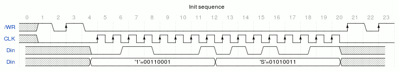
Init sequenceThe TAP can be initialised by writing to registers that have no /RESET input (most).
- NULL command
- "1S" command -> strobe the TAP internal RESET signal tied to register bit 1.
- NULL command (again : end of strobe)
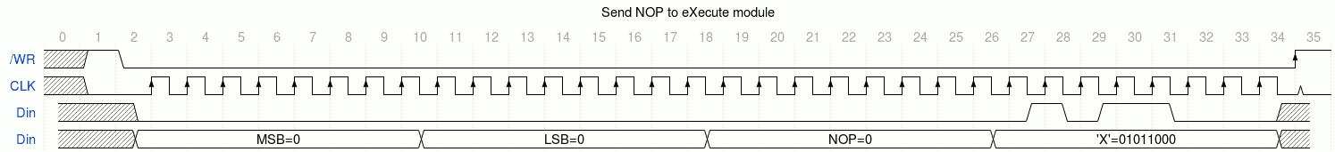
- Send NOP to Execute : 000'X' (clear the instruction register and ongoing commands)
Here is how it looks with Wavedrom:
![]()
And the last part :
![]()
.
..
. -
The TAP is coming together
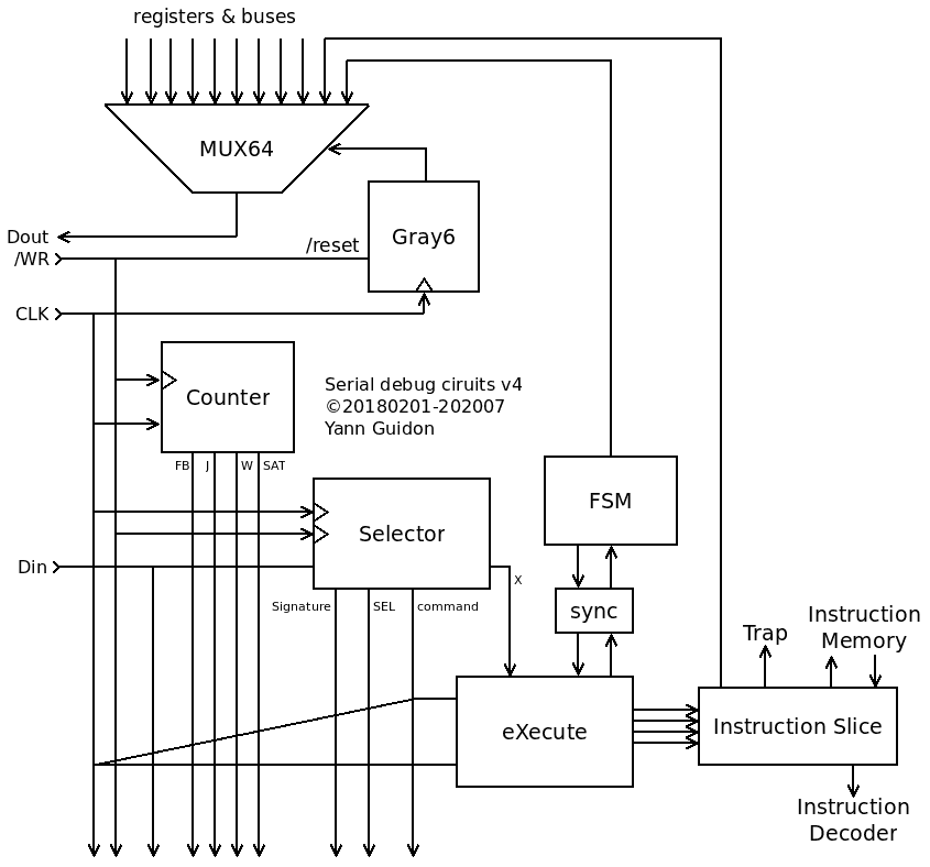
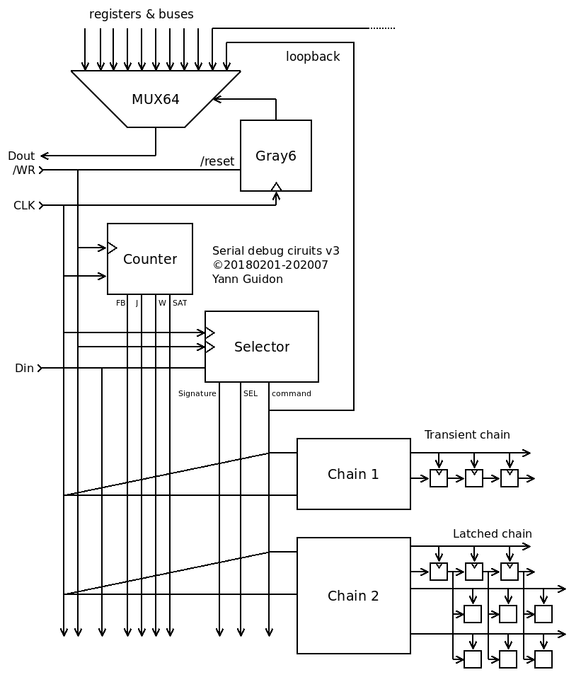
07/28/2020 at 14:36 • 0 commentsAfter about a week of intense work on the sub-parts, they are coming together as a TAP core module that lets us configure any structure at will.
![]()
The 4 sub-parts are combined to let me add chains of any length, either "transient" or latched. These chains can be very simple or with multiple checks, answer to arbitrary signatures or start at any position after the Selector's 16 bits.
Now comes the time to think about how to use it.
First possible example is to stream the program into the instruction SRAM :
- set /WR low (or send a NULL command if unsure)
- select the appropriate chain/function with the command '1S'
- toggle /WR high and low
- stream the 512 bytes of instructions
- send the signature byte (TBD) to validate the operation
- set /WR high
Reading back is something else, one has to go through the "normal path" : set PC to the address and read the instruction buffer. So how do you do that ?
Well first you have to stop the core, which means you also need to start or even step it : the Start/Step/Stop trinity is one of the messages that are sent to control the internal FSM with a command register. The FSM state is read back to confirm and acknowledge. This could go to the register address "F" for example.
But there is no "read the register" command. There is even better : the tree reads the values of the SND, SRI, Result and PC busses. All there is to do is inject an instruction in the decoder's input and not let the core record the result.
So far this chain looks like this :
- Instruction : 16 bits (MSB first)
- suffix1 : FSM state/message/command byte
- suffix2 : 'X' = 01011000
The Suffix1 byte can reuse the command register in the Selector unit. The instruction shift register can then be freely routed close to the decoder, and a MUX2 selects if the instruction comes from the TAP or the instruction memory.
The MUX2 is controlled by a single latch bit from the command byte : the whole shifted word is half-transient because the instruction doesn't need to be latched, but the command does.
-
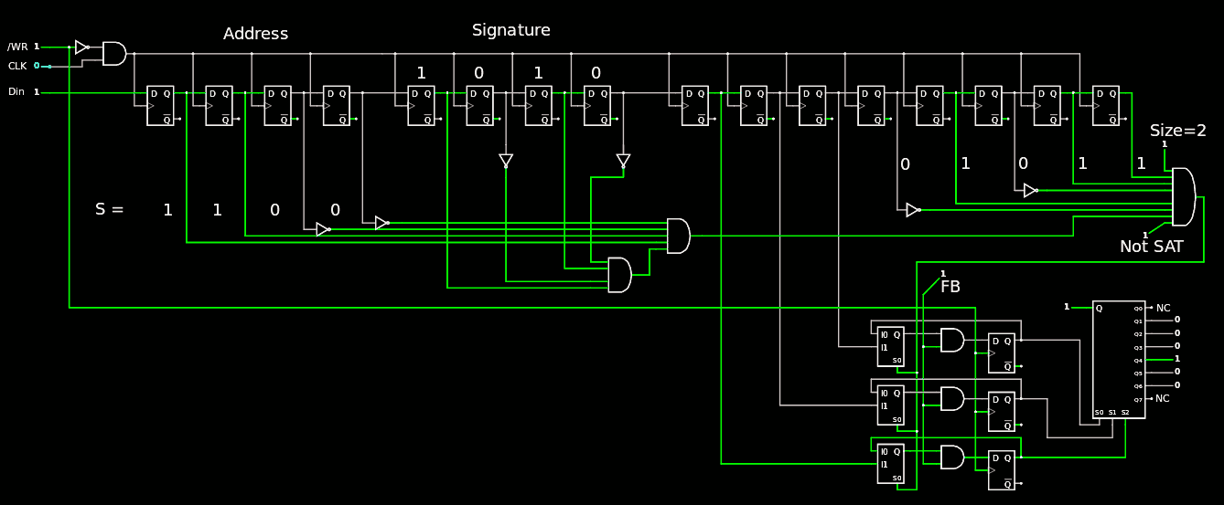
The TAP selector
07/26/2020 at 16:34 • 0 commentsAs shown in the log 111. Design of a TAP : the SIPO Controller, the first module is the "selector", used by the other modules to enable a given sub-chain or another, or none (when the "null" command is given).
A preliminary version is simulated in Falstad :
![]()
This module provides both an early signature decoder, as well as the SIPO chain for the first 16 bits, available to other modules.
The latching mechanism is also specific, unlike the latches of the other modules : if the FB (Full Byte) signal is off, then the selector register is cleared when /WR goes high. This catches most of the wrong sizes, including NULL, to prevent unwanted spurious behaviours.
The 3 cells can be replicated as needed if more outputs are required but 8 is already enough for a small circuit like the Y8. The codes 000 and 111 are avoided to further prevent spurious operations. The cell structure is unusual : a AND is inserted between the loopback MUX and the DFF, which has no /RESET input (just send an invalid command to clear). This system is fully synchronous, using 2 non-onverlapping clocks (CLK and /WR must be kept separate by the host)
Another subtlety : this module has a "permanent" output that must remain valid after more than one command, and it must be cleared by invalid commands so a DFF is used, instead of a latch. /WR is not used by the decoding logic, but other simpler modules will use latches and /WR must be decoded.
The TAP is looking better each day...
20200728 : I changed the command prefix to match the ASCII 0-7 characters :-)
-
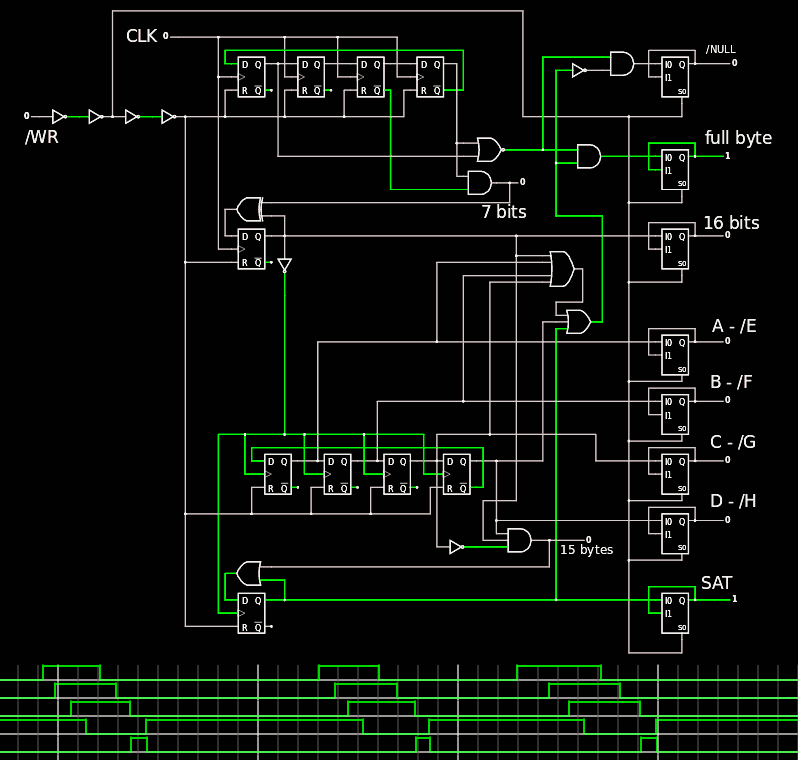
The TAP's bits counter
07/26/2020 at 02:45 • 0 comments20200808 :
This design is quite good but superseded by the TAP v2 which shares the Gray counter and saves gates. See the log 120. TAP v.2 and 122. Updated Gray Counter.
The last log 111. Design of a TAP : the SIPO Controller gives an overview of the modular structure of the TAP : the shift register can "fork" into several groups, which can be selected by writing the group number in the "S" register (it's an oversimplification).
I have spent time considering various configurations for the "stump" : apart from the shared shift register (8 bits for the signature, and 8 more for the selector), the delicate part is counting the bits while presenting useful signals despite the complicated timing constraints.
The result is the following circuit : 10 DFF, 10 logic gates and 8 T-latches.
![]()
There are 4 stages with each respective functions, and 8 output signals.
- The first stage counts the bits in a byte. When 8 bits are received, the "Full byte" signal is asserted. It shares common decoding signals with the "NULL" output which is asserted when NO bit has been received yet. It's useful for the "null" instruction : just toggle /WR low and high to clear the address register.
The counter is a simple 4-taps Johnson ring counter : it's easy to implement and requires only 2 simple logic gates for the decoding. - The 2nd stage is a simple toggle counter. The output provides the LSB of the count of received bytes.
- The next counter is another 4-taps Johnson counter to count how many 16-bits words have been received. This puts the capacity to 128 bits, which is pretty good so far. Again, the Johnson counter is chosen for its simplicity and the low logic cost for decoding : the 4 outputs require only one 2-inputs gate to select a given count.
- The last stage is simply a flag that shows that the counter has overflown. It's useful because it loops back after 128 bits and this could create protocol problems and unwanted operations...
So the order of precedence of the signals is :
- NULL on means no input at all.
- Otherwise check the "full byte" flag
- If the byte count matters, always check the SAT bit.
- Then decode the counter bits.
The following table should help :
Count
(bytes)W ABCD SAT 0 (nothing) 0 0000 0 1 1 0000 0 2 0 1000 0 3 1 1000 0 4 0 1100 0 5 1 1100 0 6 0 1110 0 7 1 1110 0 8 0 1111 0 9 1 1111 0 10 0 0111 0 11 1 0111 0 12 0 0011 0 13 1 0011 0 14 0 0001 0 15 1 0001 0 16 0 0000 1 So each module has to decode 5 bits (SAT, byte, Word, and 2 Johnson bits in Bold) to check the validity of the length, on top of the signature. It should be rather solid but still flexible and hopefully not over-engineered.
The tricky part is the timing ! This is a slow circuit so I have chosen to use some ripple-counting ideas but the devil is not on the clock signal.
All the outputs are held by transparent latches so they remain useful while the DFFs are cleared and the values are used. The /WE input is followed by buffers and explicit delays so the reset of the DFF comes after the data are latched. Otherwise it's a mess...
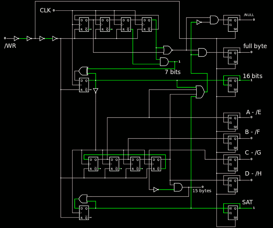
20200727 : a few minor tweaks and fixes have been devised, so it works better. I uncovered a useless race condition with the VHDL simulator and the "active" condition needs a couple fewer signals to test... The new version is available.
![]()
It should work better now ;-)
- The first stage counts the bits in a byte. When 8 bits are received, the "Full byte" signal is asserted. It shares common decoding signals with the "NULL" output which is asserted when NO bit has been received yet. It's useful for the "null" instruction : just toggle /WR low and high to clear the address register.
-
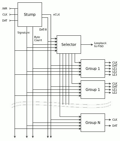
Design of a TAP : the SIPO Controller
07/24/2020 at 20:14 • 0 commentsIn the log 110. The first half of the TAP, I present the initial ideas and principles of the part of the TAP that receives data and commands.
The idea of selecting specific latches is great but comes at a significant cost : many parallel lanes make P&R harder despite the other gains. I can imagine that data must be sent at various places of the chip and that would also interfere with routing. One or two wires, not a problem, but 8 or 16 become annoying. 2 or 3 latches per DFF would be the most that is reasonably possible, depending on the circuit. Some may accept only 1 latch...
Thus it becomes necessary to split or "fork" the shift register chain. Not just the Group Latch Enable signals but also the clock signal (which also reduces the load on these signals). This is more complicated because the clock signal must be enabled before the data get shifted in and a suffix approach doesn't work. A prefix becomes necessary but it is not practical because setup&hold (and timing in general) would make the decoding logic too hard.
A "control word" must be received as a preliminary to set the appropriate latches. I choose the signature S=01010011 (nice one !) to select the address register, which can be a single byte as well. Total : 16 bits to shift in before /WR is pulsed again.
And now we see another safety feature that can be added to enforce the protocol : check the number of received bytes (yes, bytes, so it's easy to drive from a microcontroller's peripheral for example).
- We want to ensure that the number of bits is a multiple of 8 : a 4-taps Johnson counter is appropriate (only one AND2 gate for the logic).
- We want to know if the number of bytes is odd or even : another DFF gets inverted when the above counter overflows.
- Some commands want to get a higher number of bytes so another 4-taps Johnson counter can predecode the appropriate control signals.
total : 9 DFF and minimal logic to drive other decoders. It could be fewer but it's reasonably expandable for a 8-bits CPU.
We can also detect a "Null" command, where /WR is toggled on and off without touching the clock or data signals. This will reset the selector, for example, to ensure that new commands get delivered to the right chain.
But now that we can select which sub-chain gets shifted, we have more choices :
- Drive 2 or 3 latches from 1 DFF, using as many Latch Enable as required (and some decoders).
- Drop the latches altogether and only use the clock signal, when the value is "transient" (shifting doesn't cause problems because the core is on hold or the data is not required until after the command is finished) => these limited cases would be very easy to route because only 2 signals (data and clock) need to be routed.
So the "core" SIPO circuit contains the counters and the shift register for the signature.
An additional module will check for the signature then latch an address, that is then decoded to select other modules, which may drive one chain, or a chain and other latches. The overall architecture looks like this :
![]()
This makes the VHDL easy to write and flexible : new chains can be added as needed, or lengthened, some chains can be validated by a signature and/or a length... A whole vocabulary can be built from these generic modules.
There is however always one last byte to shift into the "stump" (after all the actual data) where the signature is held to be compared as a last check.
YGREC8
A byte-wide stripped-down version of the YGREC16 architecture