David Scholten
-
Goodies from the Internet
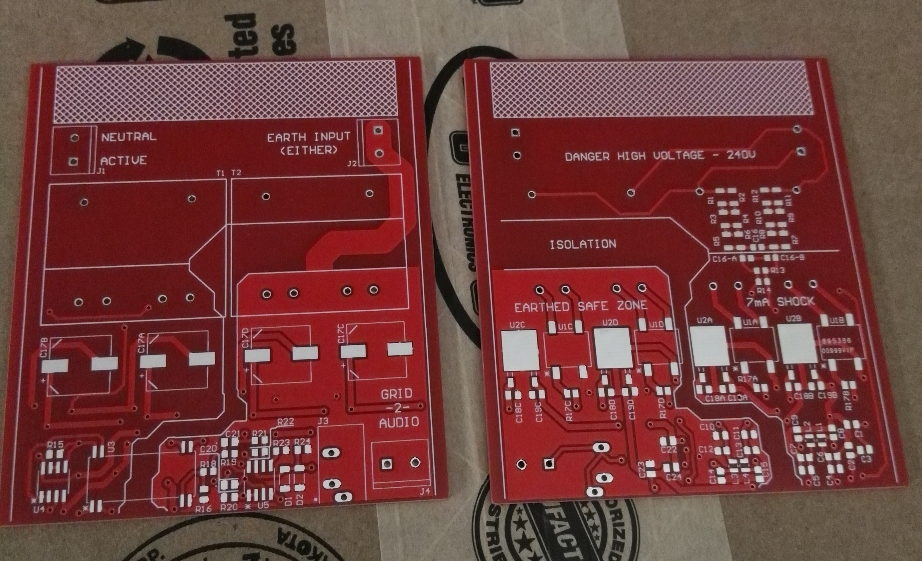
09/06/2018 at 02:39 • 0 commentsAlthough, yes, the first version of the PCBs had design issues and are not usable (notice J3 is NOT slotted), they arrived in good order and seem to be quite alright. Here is version 1.0 at last:
![]()
![]()
Labelling the entire bill-of-materials for the PCB did take some time though (transformers not shown):
![]()
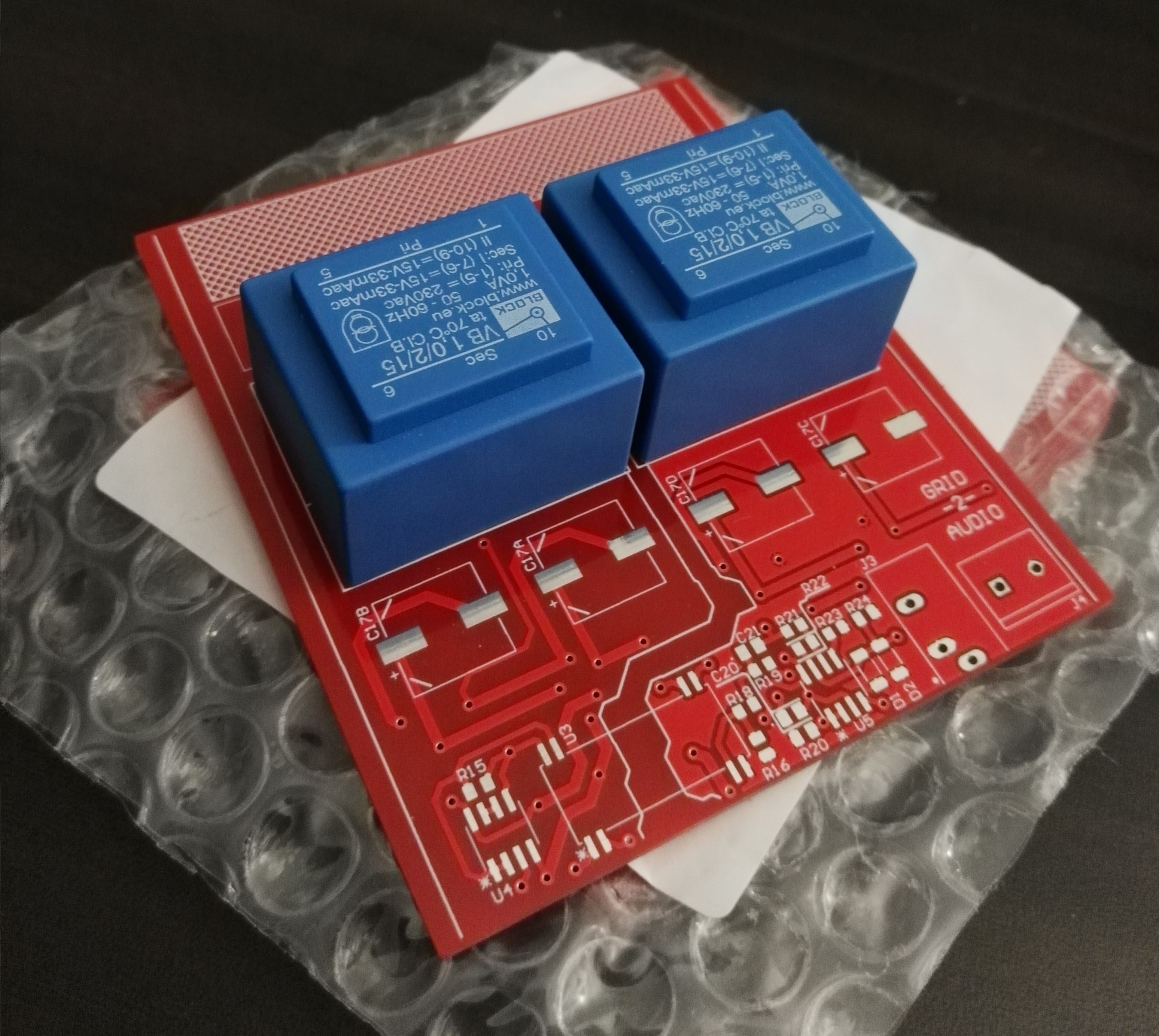
As the PCBs are so cheap compared with a set of components, I will certainly not be soldering together V1.0 and instead opted for express shipping for V2.0 of the PCB (ordered on the 2nd Sept.).
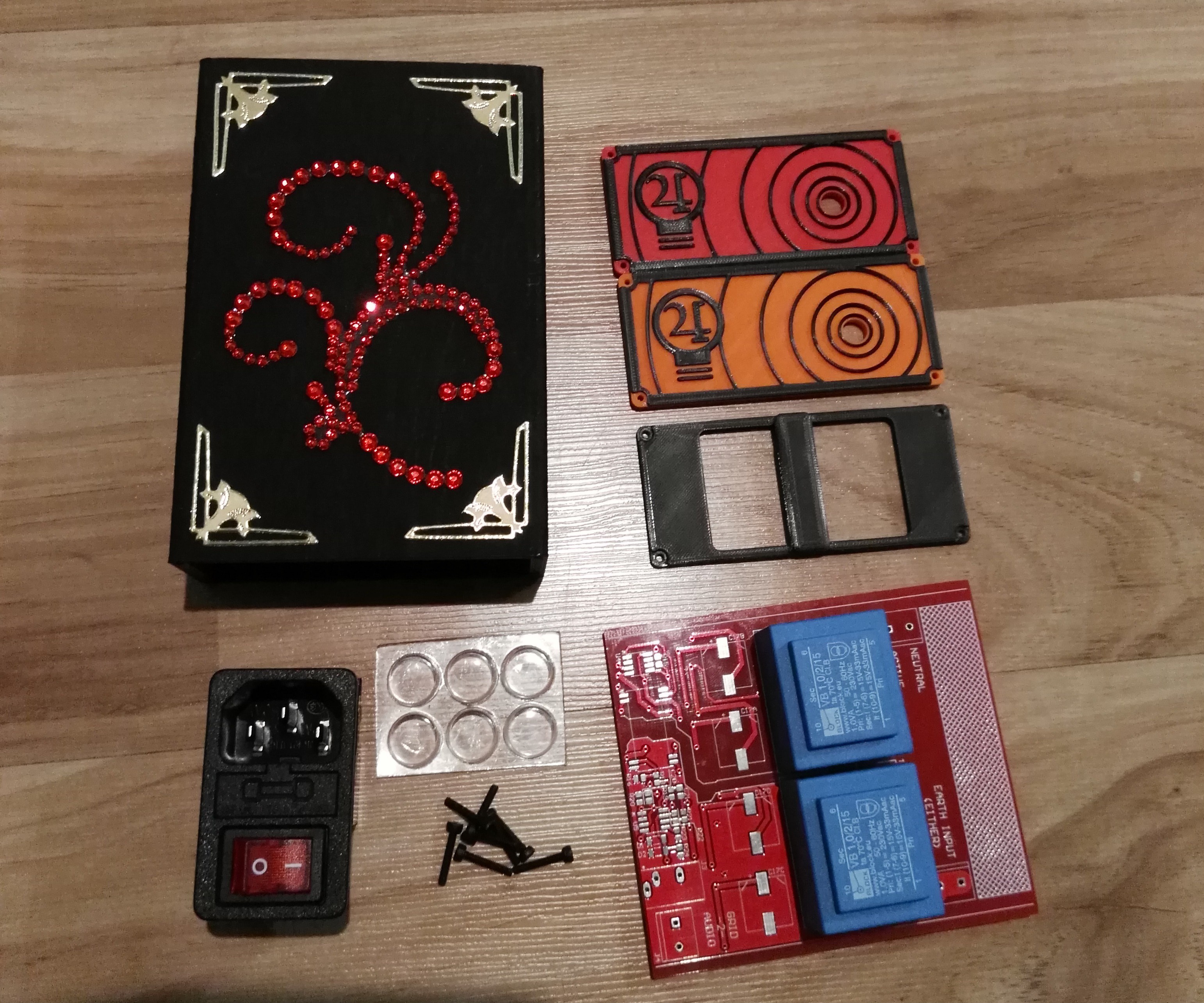
I did have fun preparing and decorating the enclosure parts though:
![]()
Though I'm still having trouble choosing between the red and orange face plates...
Project status:
Sorry for the small update, a larger one is coming soon that will include an upload of all of the CAD files to allow others to do whatever they like with them (short of commercial use). Additionally, there will be a more detailed explanation of the v1.0-->V2.0 changes as well as an upload "final" schematic project photos.
-
Cya Later Prototypes Cases!
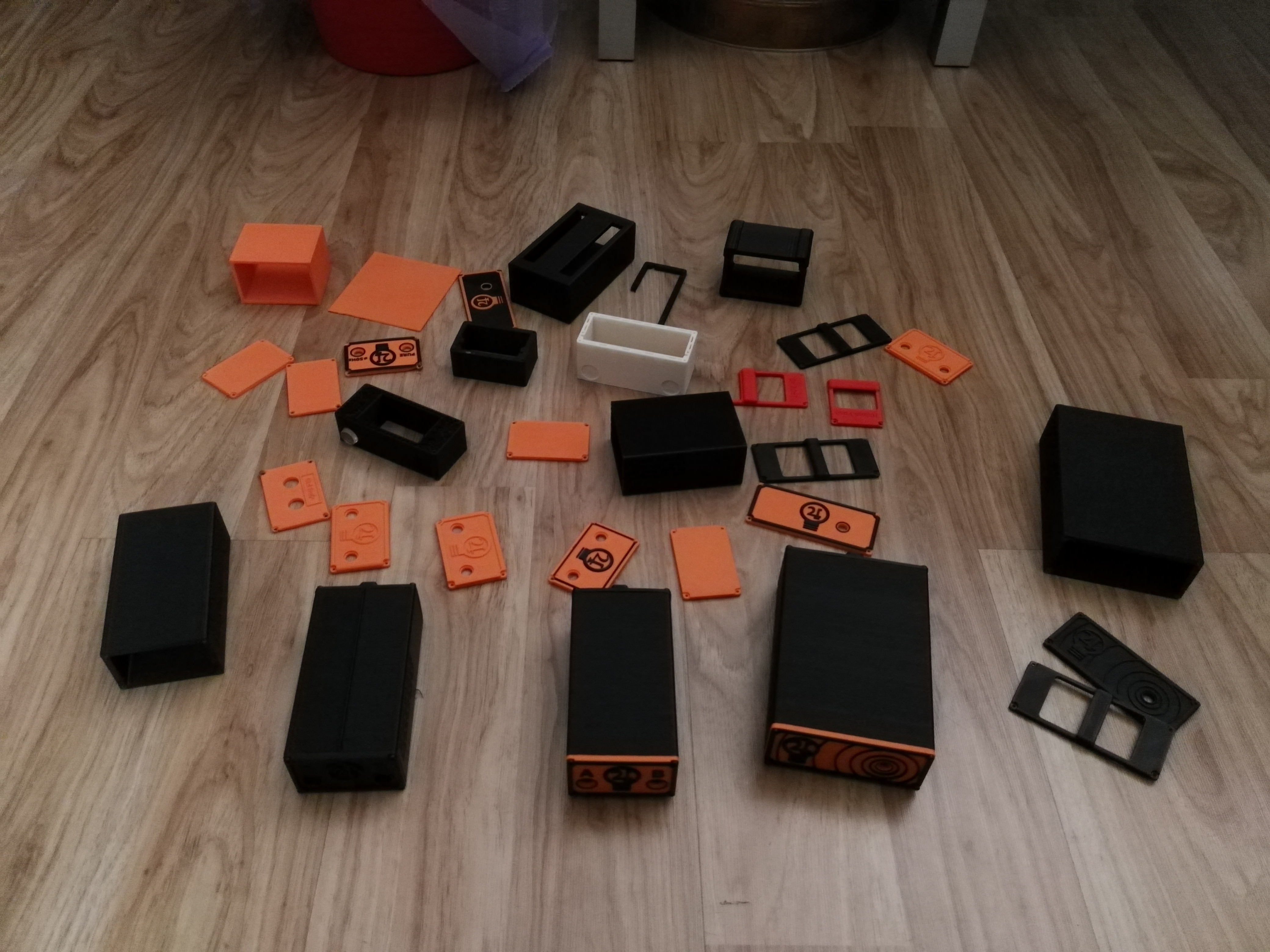
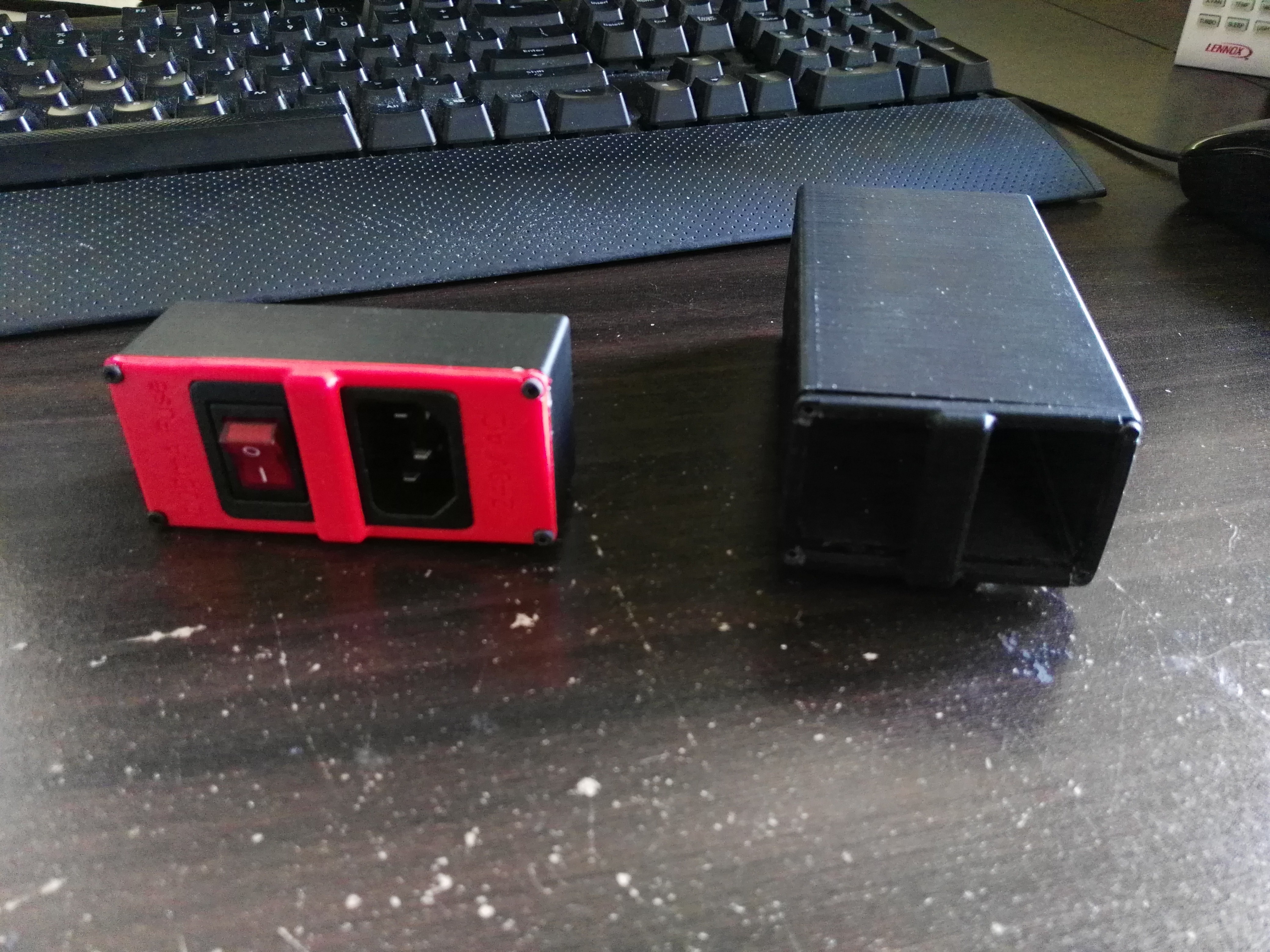
08/14/2018 at 12:58 • 0 commentsIt's been quite the 3d printing adventure, but it's time for the pieces of prototype cases to finally go in the bin (save for the few nice looking ones at the bottom):
![]()
-
The End of the Design Phase!
08/06/2018 at 06:42 • 0 commentsSo here's the latest update!
After a break from the project, I've had some time to finalise all of the minor aspects of the PCB layout (connectors, spacing, physical dimensions, etc.) It took an entire day, but putting it off would have taken an entire month.
This is, without a doubt, the final high-level circuit diagram:
![]()
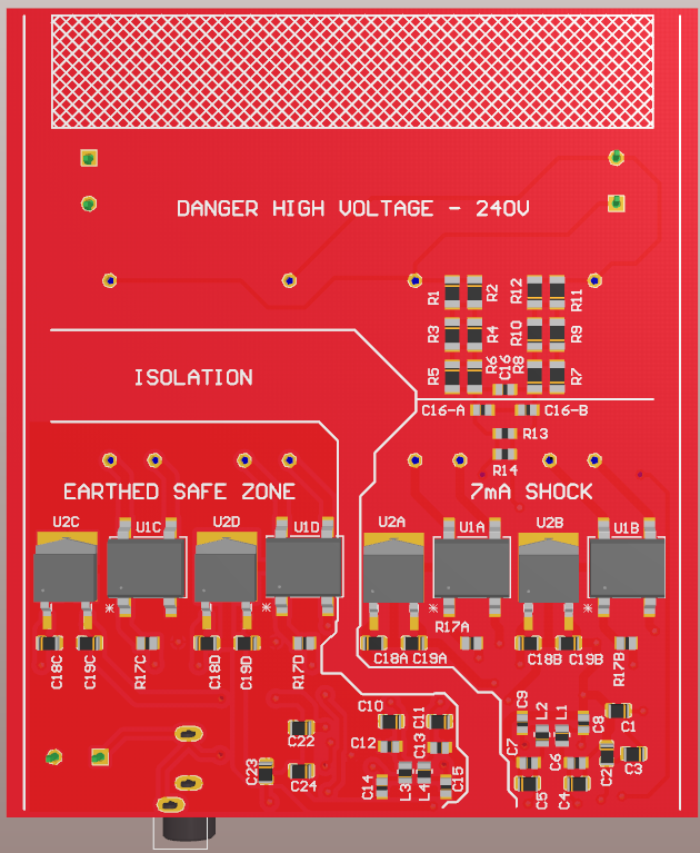
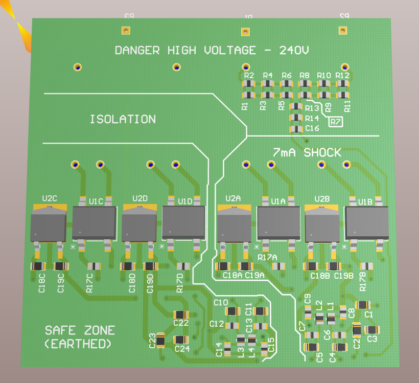
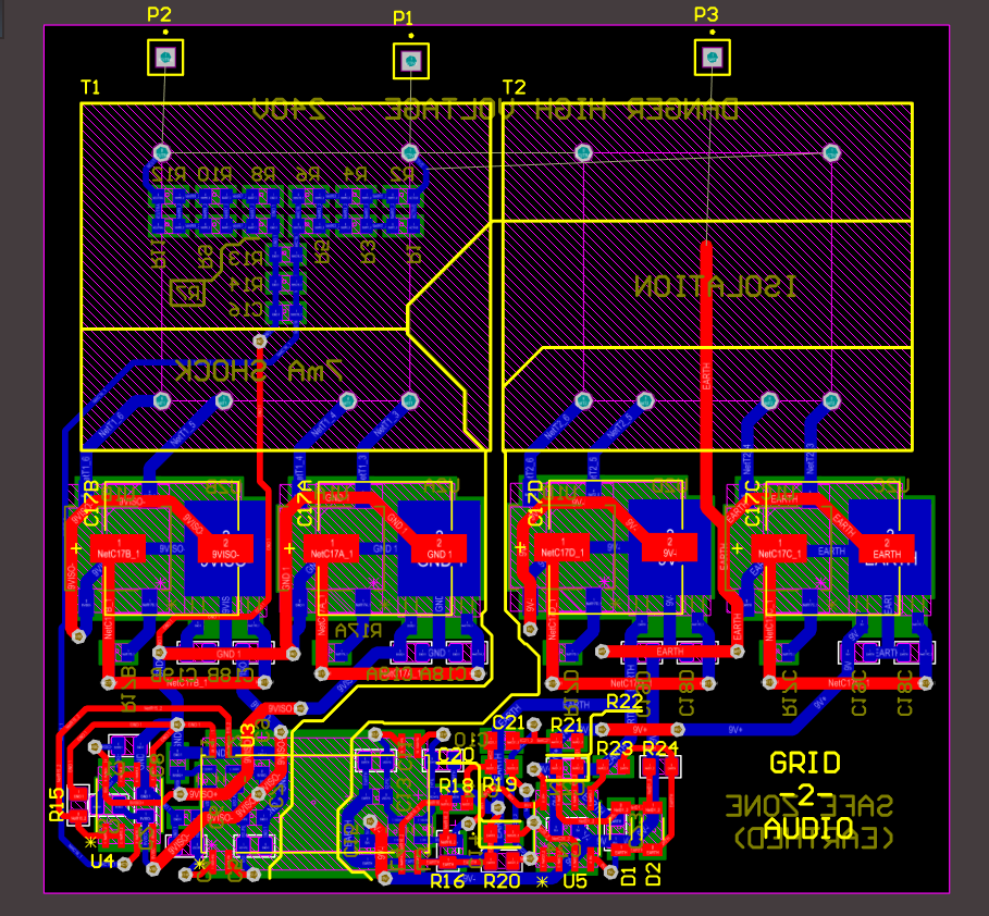
The final layout:
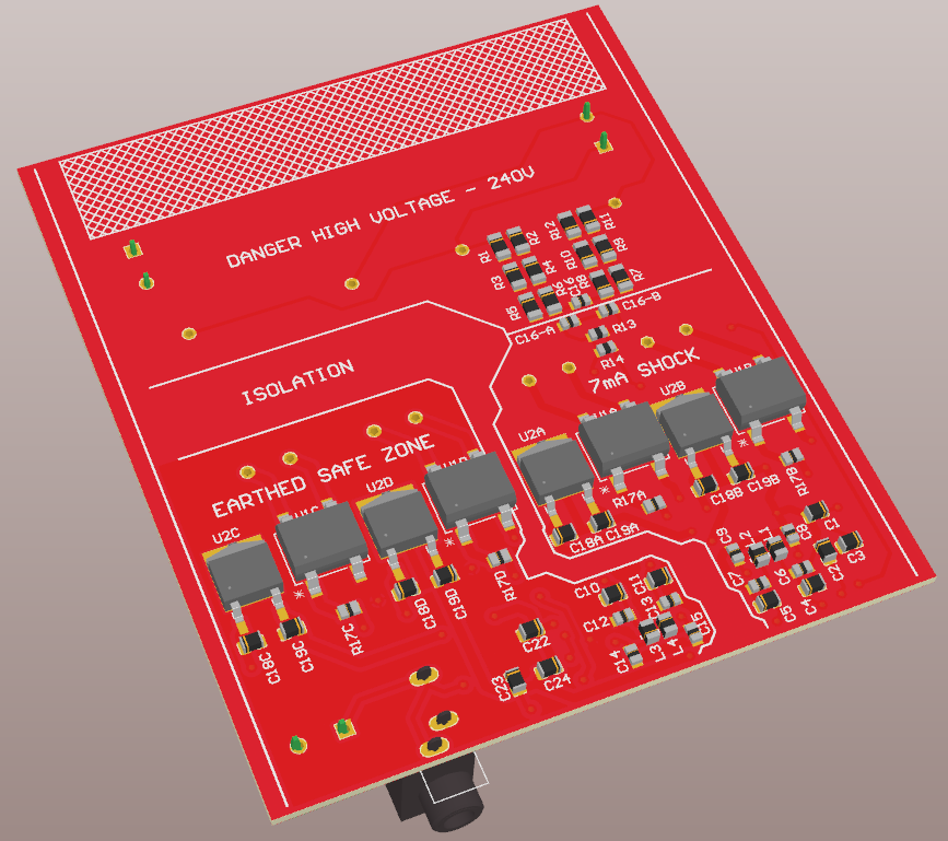
![]() I did have some concern about the spacing between the "7mA Shock" section and the "safe" section, which is only separated by 2.5mm at the closest point. I was under the assumption that 7mA through the human hand to ground was merely painful, but it seems to start to encroach in the "cannot let go" territory. As a precaution, I've made a few circuit modifications to allow a sensing resistor configuration that will only allow a current of 3-4mA (max) through the human body should something go wrong (60kOhm inline resistance). However, for this to possibly occur, four things would have to happen:
I did have some concern about the spacing between the "7mA Shock" section and the "safe" section, which is only separated by 2.5mm at the closest point. I was under the assumption that 7mA through the human hand to ground was merely painful, but it seems to start to encroach in the "cannot let go" territory. As a precaution, I've made a few circuit modifications to allow a sensing resistor configuration that will only allow a current of 3-4mA (max) through the human body should something go wrong (60kOhm inline resistance). However, for this to possibly occur, four things would have to happen:
-->The 2.5mm isolation is breached.
-->Earth comes loose within the unit.
-->The connected 3.5mm device also has an unearthed ground.
-->The person has conductive hands, etc.
Although unlikely, this is still concerning, especially if I were to give/sell a unit to someone else.
Regardless, back to snappys:![]()
![]()
![]()
![]() The idea behind the white silkscreen section at the top and the terminal blocks up there is that in this way an IEC quick connect panel mount connector can be used at the end of the case to make the PCB into a single unit (as originally intended). However, this also allows the PCB to be removed from the 3D printed case and used as a separate mains-->audio PCB as part of a bigger unit (with terminal block input/output). This is also the reason for the terminal block next to the headphone jack, which cannot be normally accessed whilst inside the 3D printed case.
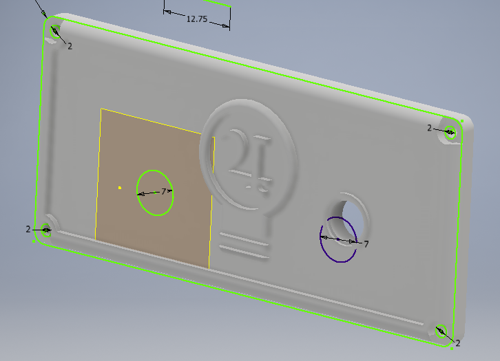
The idea behind the white silkscreen section at the top and the terminal blocks up there is that in this way an IEC quick connect panel mount connector can be used at the end of the case to make the PCB into a single unit (as originally intended). However, this also allows the PCB to be removed from the 3D printed case and used as a separate mains-->audio PCB as part of a bigger unit (with terminal block input/output). This is also the reason for the terminal block next to the headphone jack, which cannot be normally accessed whilst inside the 3D printed case.To incorporate the finalised PCB into the old case, the 3D printed design needs to be enlarged by about 60%.
Below can be seen an enlarged version of the primary case extrusion:![]()
However, since we're 3D printing and not actually extruding aluminium, the case body can vary in width along its length! The base of the case has a smaller opening to allow the existing IEC connector to retain compatibility:![]()
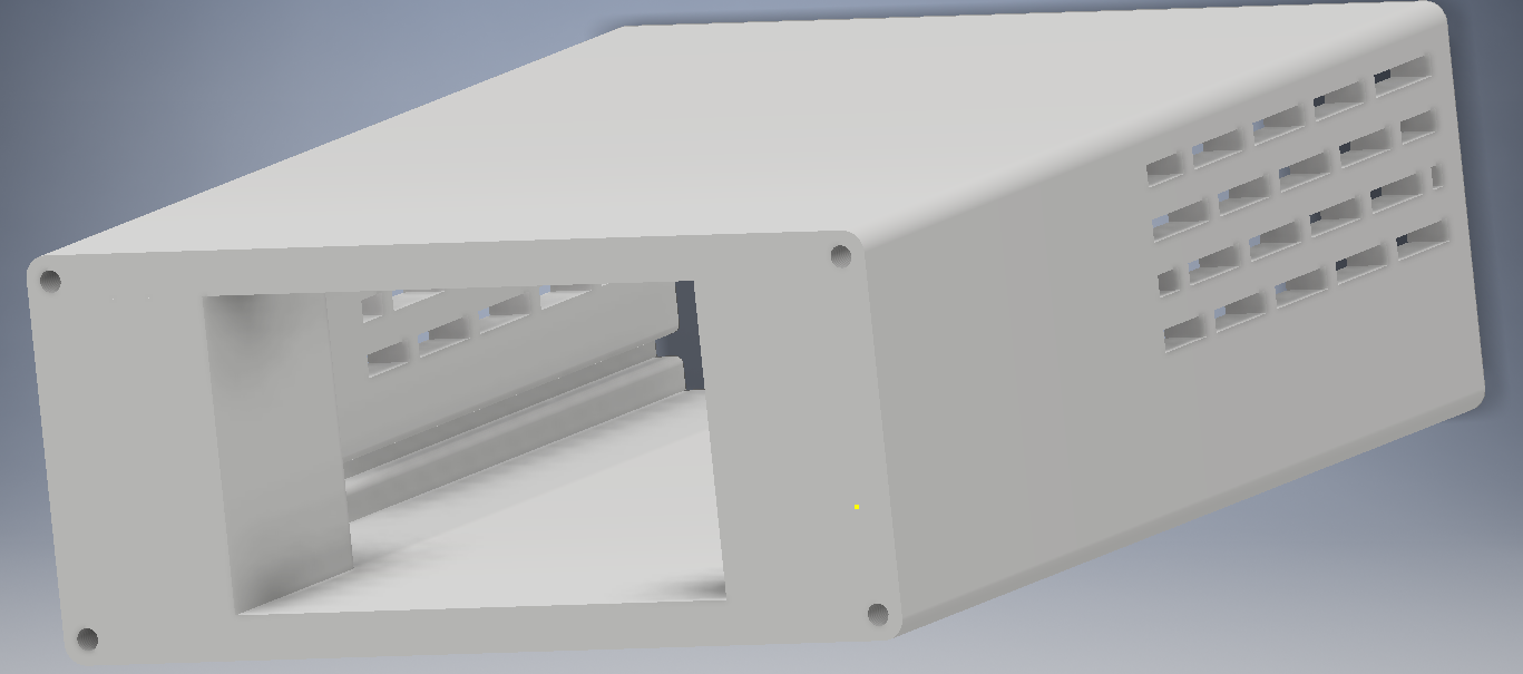
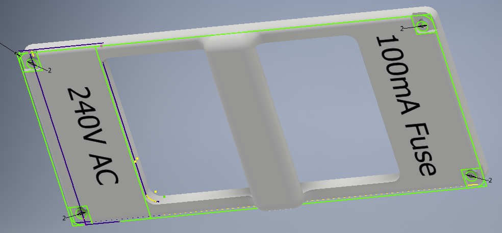
The same size expansion has been applied to the front and back panels as well, though the face decorations/labels are yet to be determined:![]()
![]()
Here's a quick picture from a failed print to preview the size compared with the old case:
![]()
I'm really feeling the project fatigue now. I've been dedicating mind-space to this project for months now and there are so many other things I want to do! Having a "properly" done PCB design and case is nice an all, but the gimmick wares off VERY quickly. This project should be called "An exercise in engineering design: tolerance and perseverance" or something along those lines. I just want to breadboard sparkly things...
Anyway, the next step now is to print all of the cases to a satisfactory standard and make an order for the PCBs/components. Ideally everything will fit and the PCB will work fantastically the first time it's powered on.
I'm sure this will be the case...
-
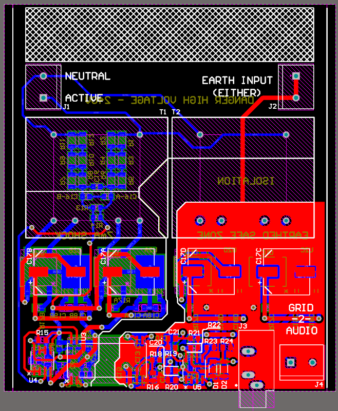
PCB Layout
07/13/2018 at 01:15 • 0 commentsAs promised, here is the PCB layout of the Grid-2-Audio module (minus the I/O connectors).
Top view:
![]()
Bottom view:
![]()
2D view:
![]()
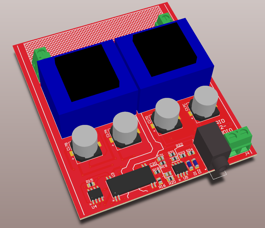
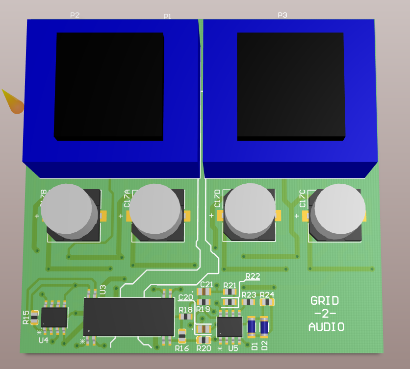
The general philosophy was to divide the board up into three sections, each with an escalating level of danger. The first is the mains section, which exists solely to power the transformers and take a voltage divider. The second is the non-isolated side of the ISO124, which is powered by one of the two transformers and has a 30kOhm connection to active (about a 7mA shock potential). The third section is the isolated side of the ISO124 that is powered by the other of the two transformers. This side is effectively galvanically isolated, physically separated and earthed (earthing is not yet shown in the images).
My only concern at this point is the heat dissipation on the mains side resistive divider and the earthing circulation currents that may degrade the output signal (unlikely).
The next step is to touch up the layout a little bit and get to work on modifying the enclosure to fit the now-larger PCB.
-
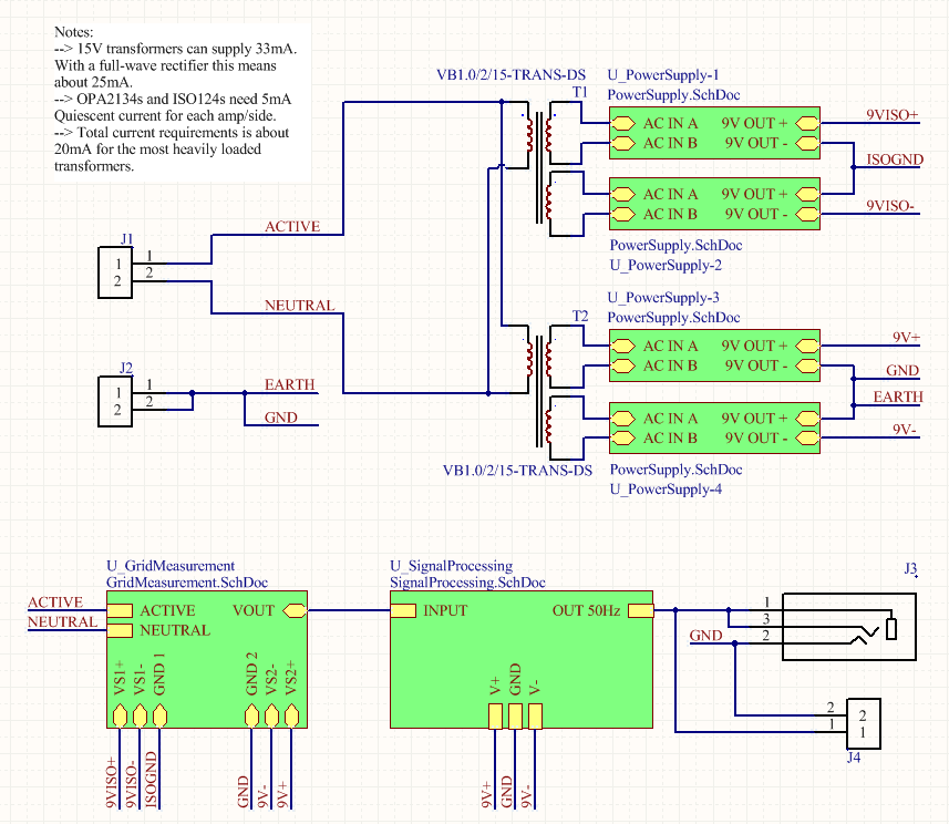
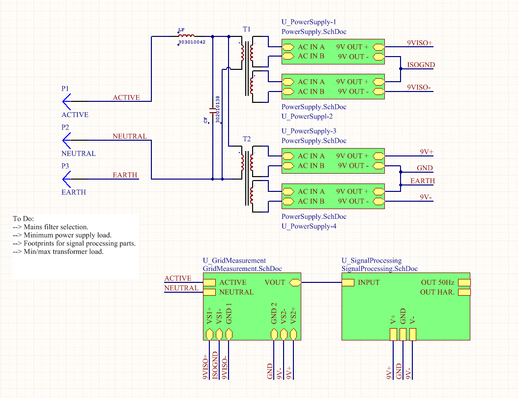
Schematic Modifications - Final Revision
07/12/2018 at 07:21 • 0 commentsSorry it's been a while, the project is still underway!
Aside from the input/output connectors, the schematic is completely finished (I know this is true this time because the layout is almost finished).
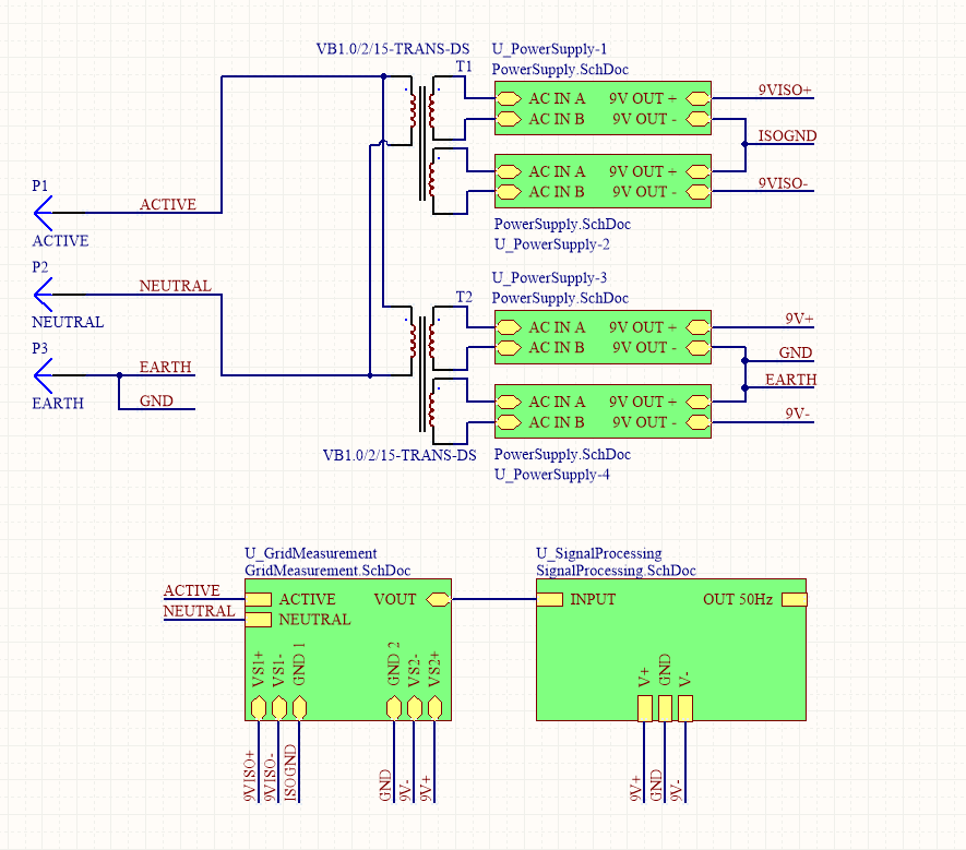
The schematic overview remains the same (minus a couple of mistakes with the power orientation):
![]()
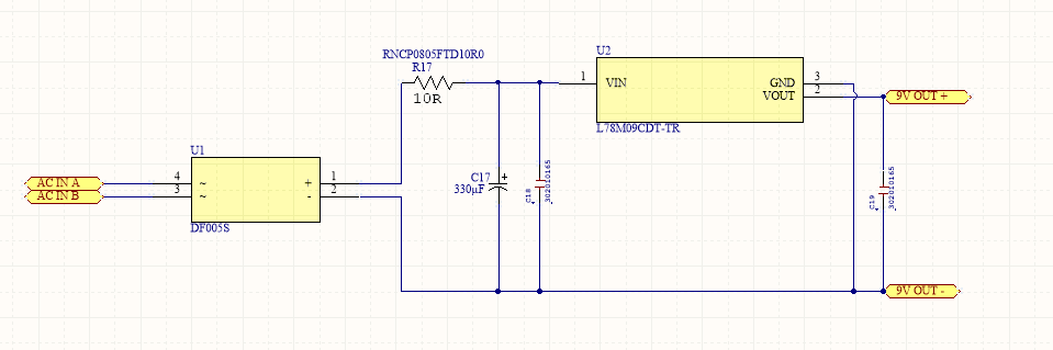
The power supplies are also unchanged (but now the wires are actually connecting and not maintaining an illusion):
![]()
The grid measurement section now contains a new input filtering capacitor (30MHz crossover):
![]()
Now, onto the actual changes... The most notable change is that the signal processing portion of the circuit has been significantly simplified to eliminate the 500Hz harmonic filter.
The original intention of this filter was to increase the dynamic range of the harmonic measurements as the available audio range is about +/- 450mV. If the harmonics are only a small portion of the 50Hz fundamental waveform, they will be at the mercy of the sound card's sampling accuracy. The secondary "harmonics only" output would eliminate the 50Hz fundamental component and allow amplification of the harmonics without the 50Hz clipping. This would then be fed to the sound card as a +/- 450mV signal to increase the dynamic range.
However, I eventually decided against this as the filter's response wasn't completely flat - Especially in the more interesting 500Hz-2kHz (10th-40th harmonics) range. Not to mention the sub-500Hz is completely gone (2nd-9th harmonic). It all seemed a bit pointless in the end.
![]()
The other change is the removal of the DC-offset removal capacitors from the op-amp U5. As the gain at this stage is 0.129 (as opposed to a value over 1.0), the DC offest from the previous stage (the ISO124's massive 20mV) is reduced to 2.57mV. As the OPA2134 will add not much more than 1-2mV, the final DC-offset will be around 5mV max in most circumstances. This is about 1% of the signal peak, which is reasonable considering sound cards block DC voltages anyway.
Now, taking these changes into account (and the existing design) the final frequency response is flat from 0Hz-20kHz and then decays from after that until about 50kHz where it drops off rapidly.
Stay tuned for the layout pics!
-
Schematics are Done!
05/30/2018 at 12:08 • 0 commentsFinally, after weeks of umming and arrring, the schematic is done!
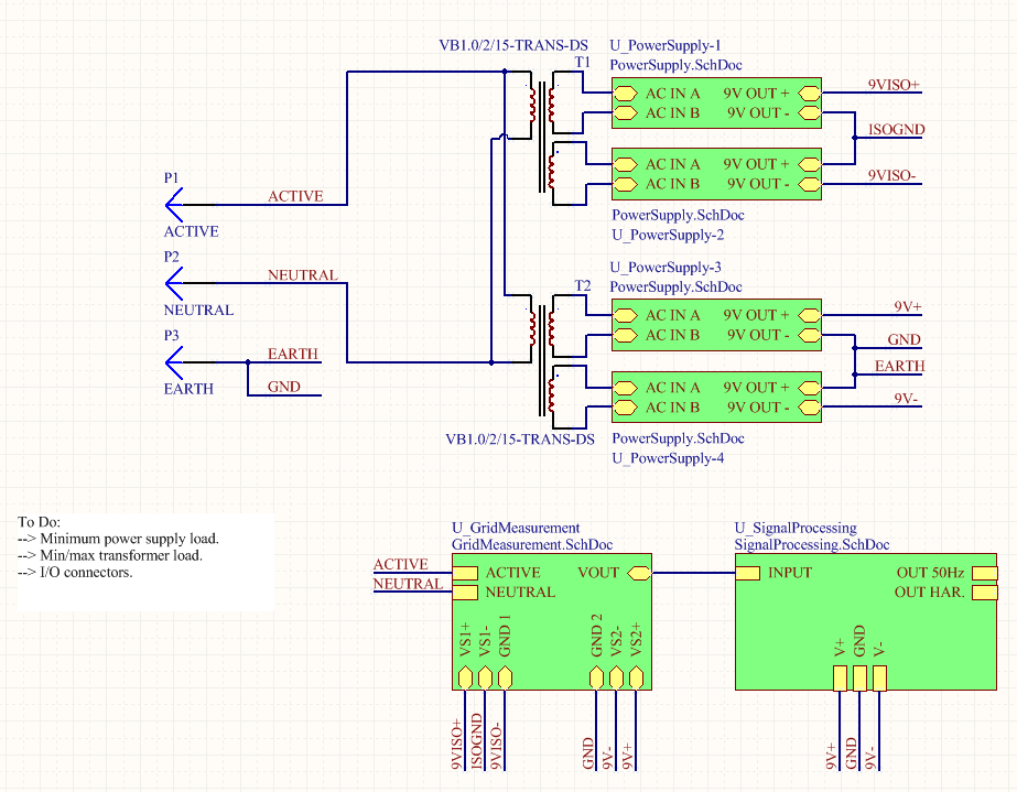
The overall design of the system has remained unchanged with the exception of the input filter. Originally, there were plans for an input LC low pass filter to reduce the harmonics and fluctuations in the mains supply current, which would result in measured voltage harmonics in the system. This is due to the resistance of the input IEC cable. Here is the final system hierarchy with the LC filter removed:
![]()
To compensate for the lack of input filtering, the power supplies have been modified to include a series resistor to limit the 100Hz “inrush” current to the electrolytic capacitor. Each half cycle there is a rush to “refill” the capacitor, which results in a sudden impulse of current. The series resistor limits this current and dramatically increases the charge time of the capacitor. This thereby reduces the peak current and the voltage harmonics due to the IEC cabling resistance. However, this does reduce the minimum capacitor voltage and the transformer turns ratio has been adjusted to compensate.
The mains current before the series resistor is added:
![]()
After the resistor is added:
![]()
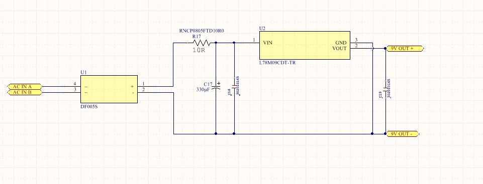
Other than this factor, the power supplies (+/-9V x2) are quite basic and remain mostly unchanged:
![]()
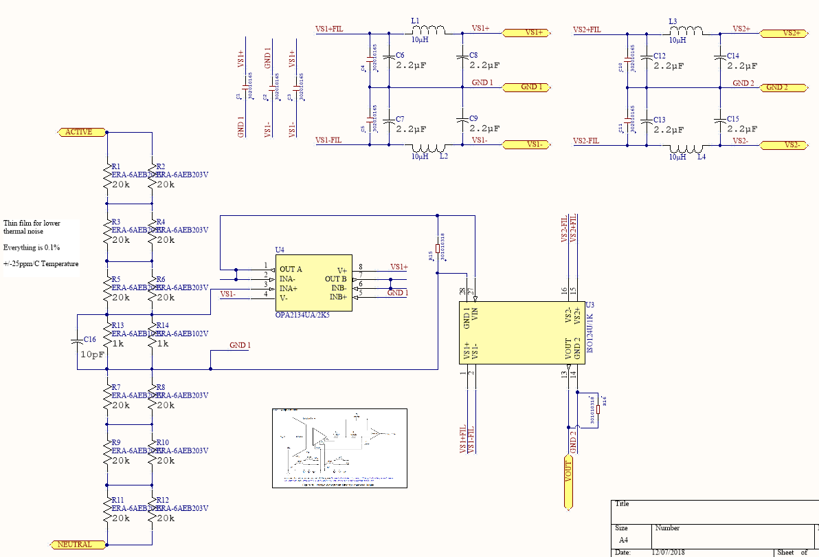
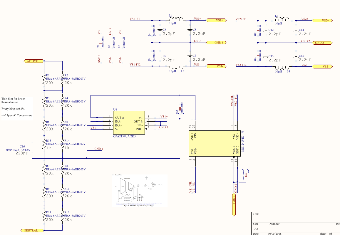
The signal acquisition block of the hierarchy takes the grid voltage and produces a safe, isolated, 4V copy to send on to the signal processing block:
![]()
First, the voltage dividers reduce the mains level down to the 4V level. Using such large value resistors (power dissipation limits) has the potential to introduce thermal noise at this point, so the thick film type resistors were used to alleviate the issue. The 4V signal is then buffered by an OPA2134 op-amp and fed to the ISO124 isolation amplifier (lower input impedance), which provides near-galvanic levels of isolation. One of the many drawbacks to the ISO124 is the practical requirement for 4 separate power supplies (two of which are isolated from the other two) to drive it. Additionally, the ISO124 leaves the signal with a 20mV (0.5%) DC offset, a very low current driving capability (<10mA) and a 10mV (0.25%) 50kHz ripple.
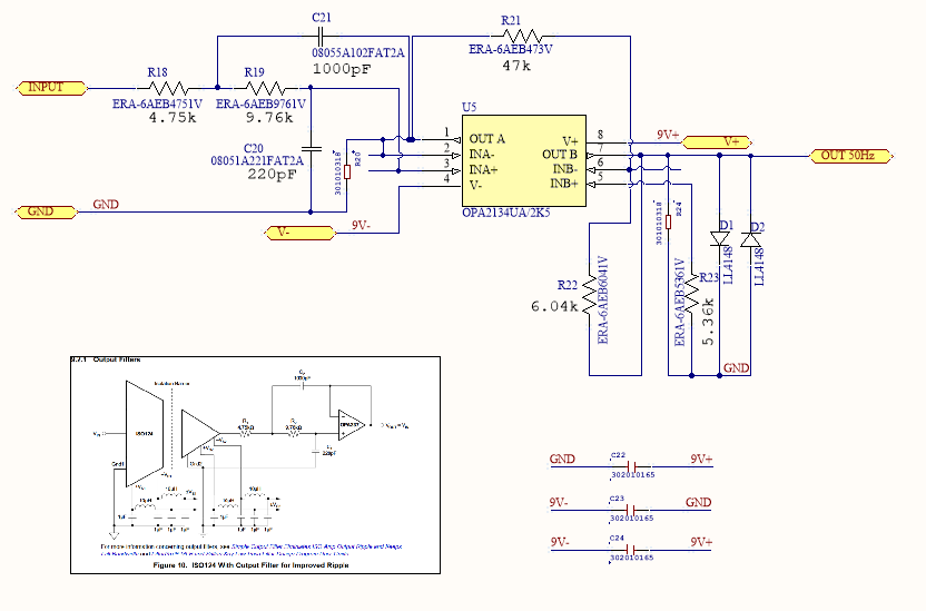
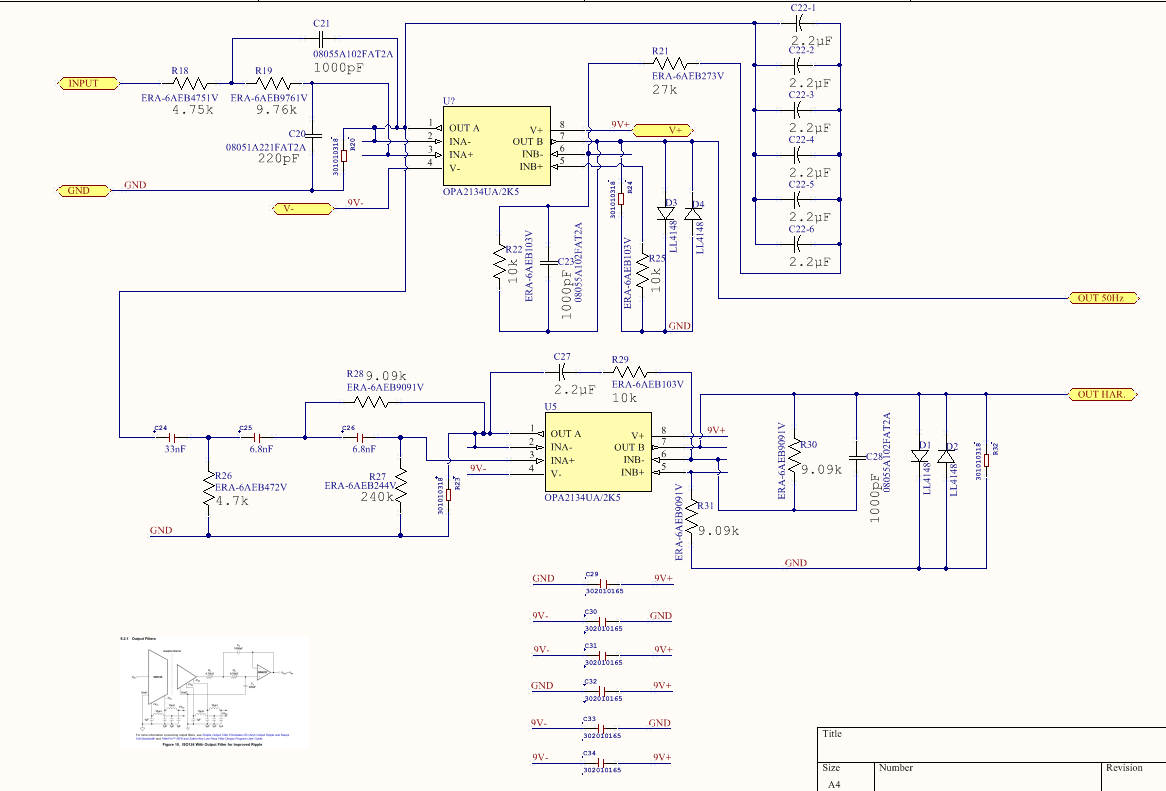
Signal processing time (some resistors and caps have not been selected):
![]()
The signal processing hierarchical block takes the 4V signal and applies a 2nd order low pass filter that works in conjunction with the internals of the ISO124 to produce a 3rd low pass filter to remove the 50khz ripple. This signal is then sent to an inverting amplifier to reduce the signal magnitude to about 450mV peak and provide increased current drive capability. In addition, this op amp also removes the DC offsets that have accumulated and removes any RF interference/noise (1.5MHz 3dB point).
The 4V signal is also sent to a 3rd order high pass filter for a harmonics only output (500Hz+). After this the harmonics-only output is sent to another op amp to increase the signal magnitude to a matching 450mV peak output (along with DC offset removal and RF reduction).
The final outputs are/will be scaled (approximately) such that:
Main output: 0-450mVp is 0-423Vp (50Hz to 20kHz)
Harmonics output: 0-450mVp is 0-20Vp (500Hz to 20kHz)
The frequency range does expand up to 50kHz (-3db), but it only remains flat until about 30kHz. As sounds cards (mostly) cap before 20kHz, I only concerned myself with the bandwidth under 20kHz during the design process.
Sorry for the incoherence throughout the post - It was written quickly in many chunks ;)
-
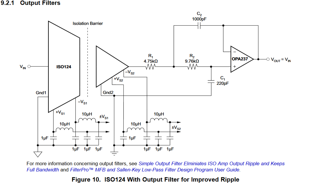
It's the Little Things...
05/05/2018 at 12:13 • 0 commentsStill working away at it in my spare time, but a lot of small things are catching me out.
The latest is the ISO124, a 21 year old IC, with extended requirements for bypassing and output filtering:
![]()
It's not that it's difficult to implement, but the assumption that it this sort of IC conditioning wouldn't be necessary is what now requires me to rework some of the design.
This IC also makes all of its electrical claims with only a 2kohm load - Do I need this?! Can I buffer the output and improve the specs - Or does it make them worse?! I'm not going to make more assumptions. Working backwards from examples gives clues, but it is frustrating.
The 2k load then has a cascading effect on the power budget and so on, which is causing continual annoyances.
More to come soon.
-
Altium Schematic Preview
04/12/2018 at 13:37 • 0 commentsI'm been making some progress on the Altium schematic!
Although mostly complete, there are a lot of annoying "Altium-y" things left to do that mostly revolve around footprint hunting and component selection.
Here is a higher level schematic that more-or-less resembles the initial sketch:
![]() The design is mostly a bunch or repeated power supplies and a signal conditioned from an isolation amplifier (not that it was going to be anything else). What is making it interesting, however, it the power restriction set by the extremely limited space in the enclosure that is forced upon me by the two 1VA transformers:
The design is mostly a bunch or repeated power supplies and a signal conditioned from an isolation amplifier (not that it was going to be anything else). What is making it interesting, however, it the power restriction set by the extremely limited space in the enclosure that is forced upon me by the two 1VA transformers:![]() I'm finding it impossible to locate a small quad-secondary transformer, which would have a higher power density compared with two lower VA dual-secondary transformers. The OPA2134 op amp (I'm using two) and ISO124 chips all demand 2k ohm loads for ideal performance, which is before any output is actually connected. This is forcing up the size of the transformers and consuming space. I'll need to invest a lot of time into both reducing the sizes of components and thinking of clever placements if I'm going to fit everything in the box (which I certainly aim to).
I'm finding it impossible to locate a small quad-secondary transformer, which would have a higher power density compared with two lower VA dual-secondary transformers. The OPA2134 op amp (I'm using two) and ISO124 chips all demand 2k ohm loads for ideal performance, which is before any output is actually connected. This is forcing up the size of the transformers and consuming space. I'll need to invest a lot of time into both reducing the sizes of components and thinking of clever placements if I'm going to fit everything in the box (which I certainly aim to).
I think this is going to be a fun layout! -
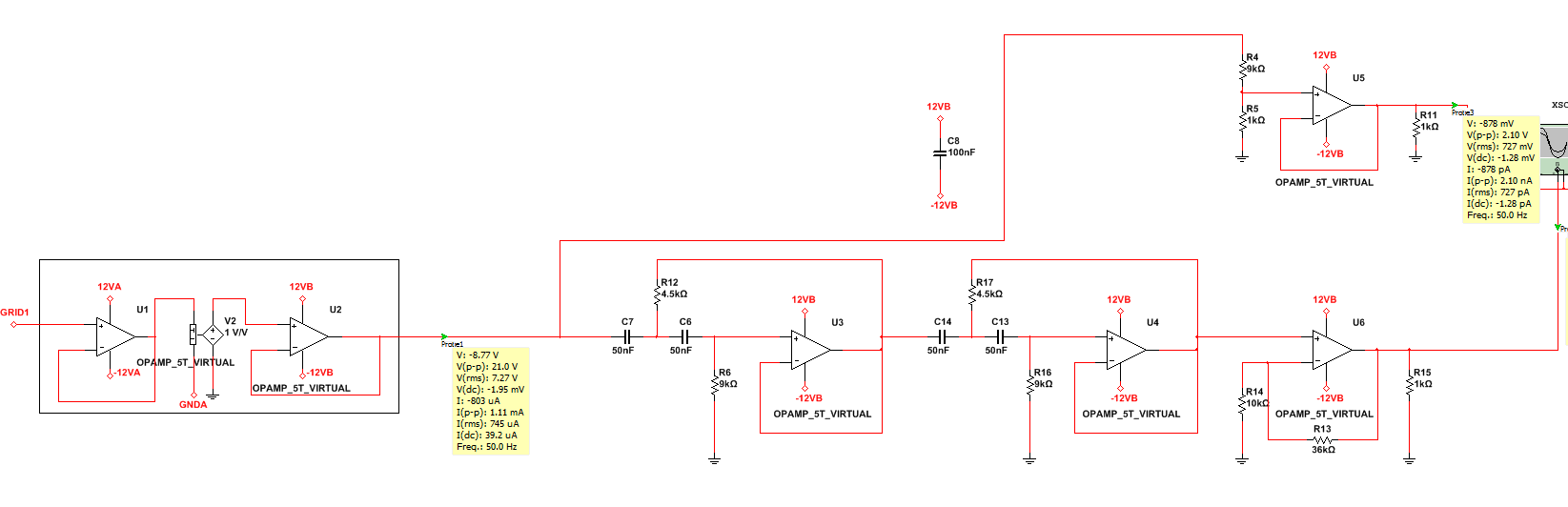
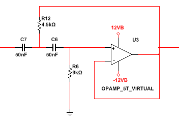
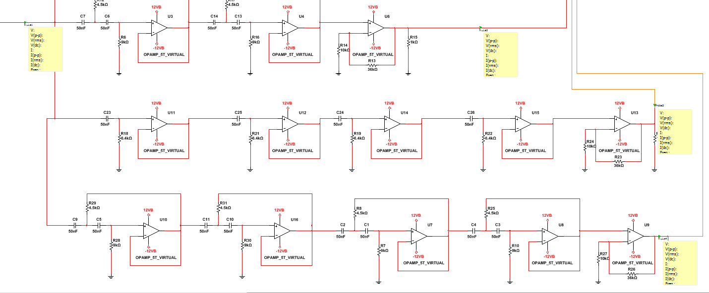
Circuit Simulations Complete
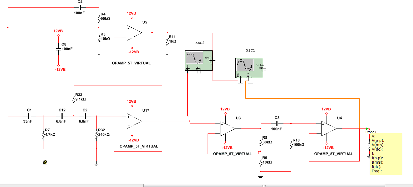
03/31/2018 at 08:32 • 0 commentsAfter an afternoon pretending that I know how to design third order op-amp filters, I settled on the following for the harmonics filter with the help of a web tool (http://sim.okawa-denshi.jp/en/Fkeisan.htm):
![]()
This tool helped with the design of the following:
![]()
Ignoring the op amp at the top, the bottom three perform the following functions (in order):
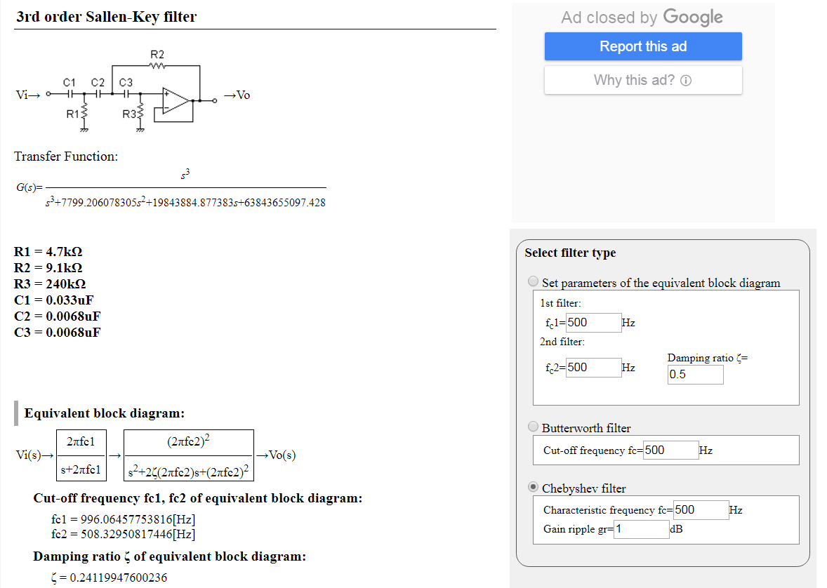
-->Third order high pass filter -->Voltage gain -->Offset removal and buffer.The third order filter is a Sallen-key type set up as a Chebyshev style with a cutoff frequency of 500Hz and a 1dB oscillation at the higher frequencies:
![]()
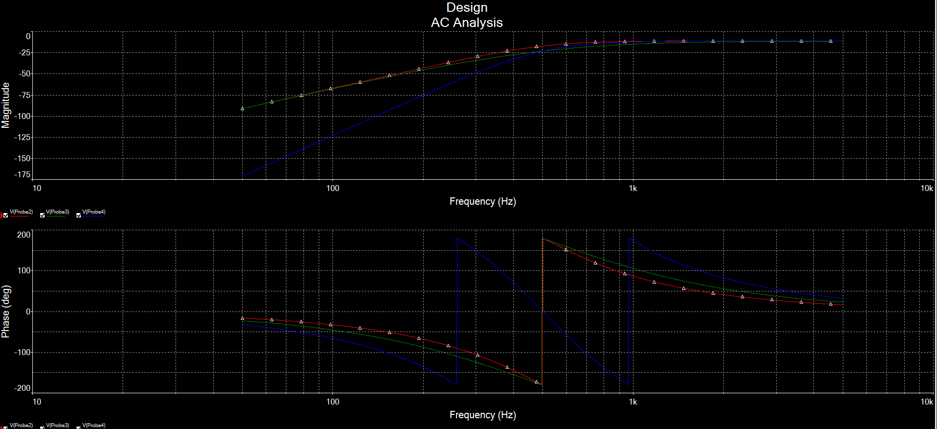
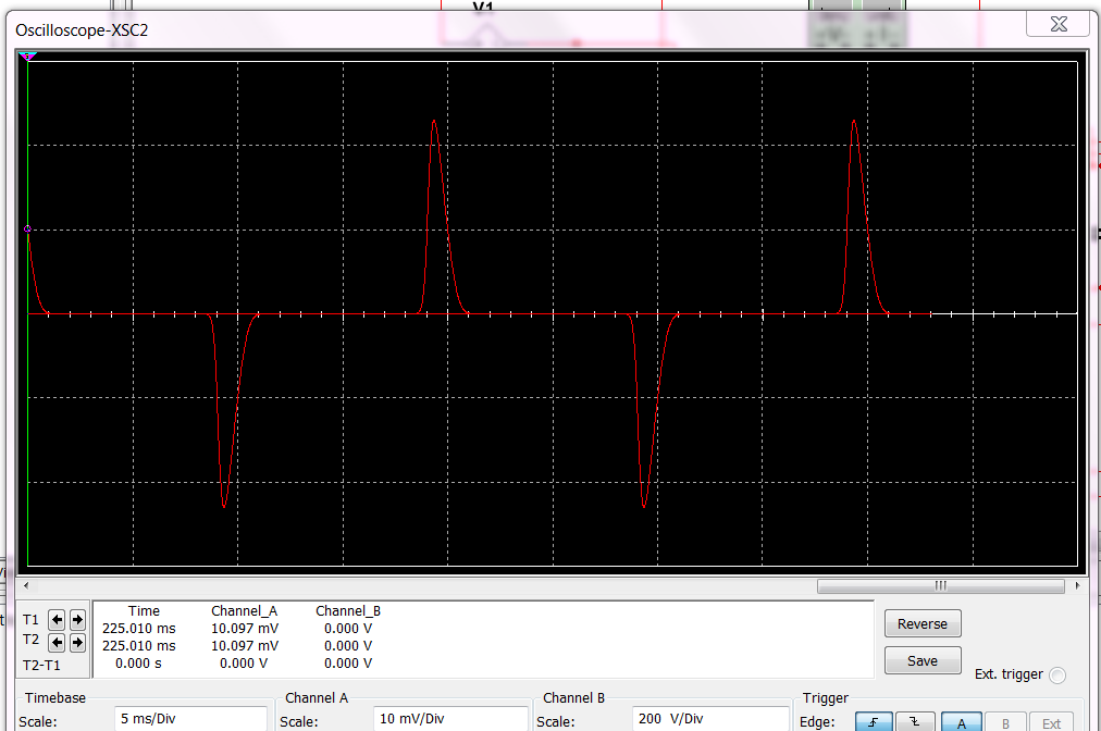
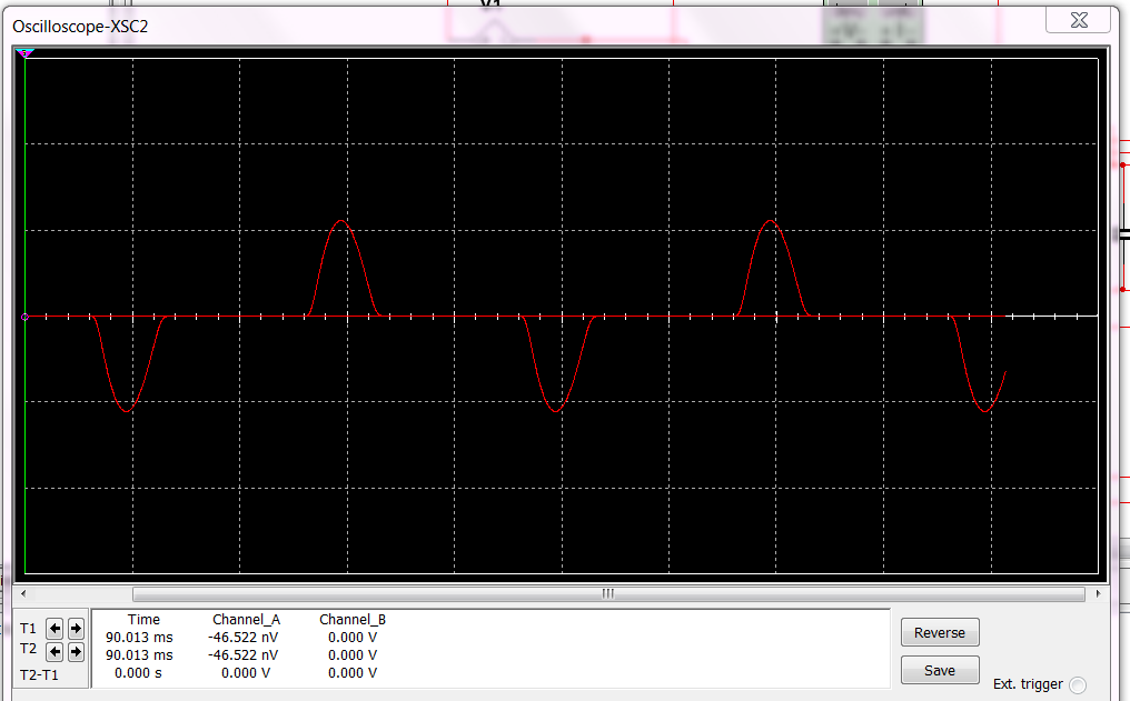
Now, with both the main signal of the grid and the harmonics (500Hz) set to the correct 1Vpp levels for sound card audio (assuming a maximum grid harmonic distortion of 5%), the two output signals look as followed on a virtual scope:
![]()
Within the actual "harmonics" output itself, the grid rejection of the 50Hz signal is -60dB (a one thousandth), but as the fundamental component is 20 times the maximum harmonic level, the practical 50Hz signal in the harmonics signal will be 1/50 (i.e. -24dB) compared with the harmonics waveform.
The next step is creating the Altium schematic and layout (or as I like to call it: The "design by whatever footprint library is available" technique). -
Circuit Simulations
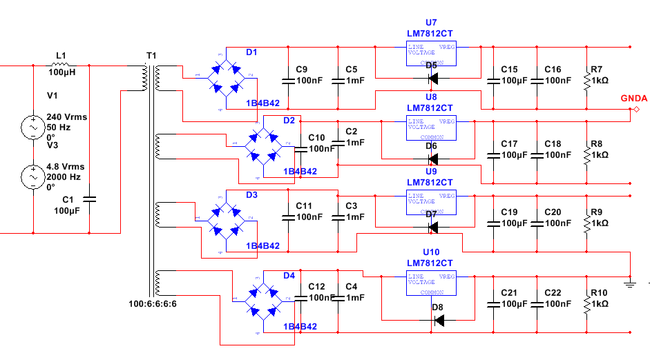
03/31/2018 at 03:15 • 0 commentsFinally had some time to get to work on the circuit design! First off is a tentative power supply with an input filter to ensure harmonics from the grid are minimised:
![]()
Taken from a resistive divider on the grid side, voltage measurements are then passed through an isolation amplifier to some op-amp stages for signal processing and buffering:
![]()
A standard active 2nd-order high pass op-amp filter:
![]()
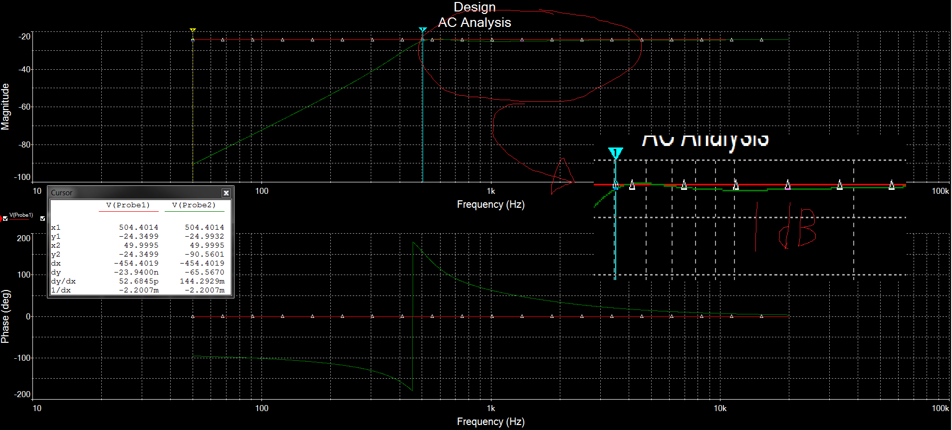
Having some fun with filters and nifty AC analysis functions in Multisim 12:
![]()
![]()
Starting to have some fun with this after all!
Grid-2-Audio
A convenient adapter to view the electrical grid waveform through your PC's sound card.

 I did have some concern about the spacing between the "7mA Shock" section and the "safe" section, which is only separated by 2.5mm at the closest point. I was under the assumption that 7mA through the human hand to ground was merely painful, but it seems to start to encroach in the "cannot let go" territory. As a precaution, I've made a few circuit modifications to allow a sensing resistor configuration that will only allow a current of 3-4mA (max) through the human body should something go wrong (60kOhm inline resistance). However, for this to possibly occur, four things would have to happen:
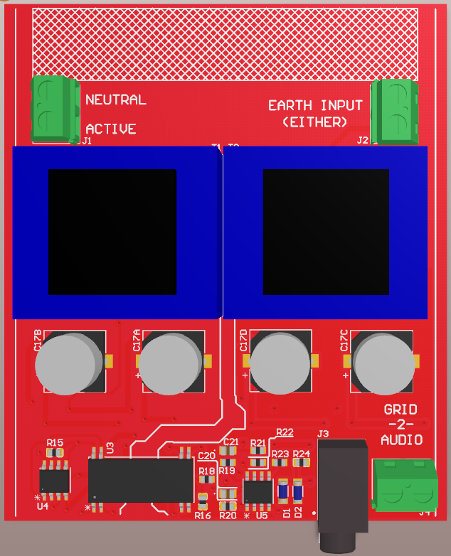
 The idea behind the white silkscreen section at the top and the terminal blocks up there is that in this way an IEC quick connect panel mount connector can be used at the end of the case to make the PCB into a single unit (as originally intended). However, this also allows the PCB to be removed from the 3D printed case and used as a separate mains-->audio PCB as part of a bigger unit (with terminal block input/output). This is also the reason for the terminal block next to the headphone jack, which cannot be normally accessed whilst inside the 3D printed case.
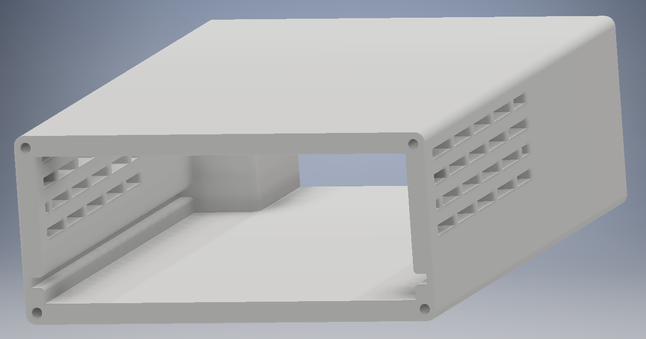
 The design is mostly a bunch or repeated power supplies and a signal conditioned from an isolation amplifier (not that it was going to be anything else). What is making it interesting, however, it the power restriction set by the extremely limited space in the enclosure that is forced upon me by the two 1VA transformers:
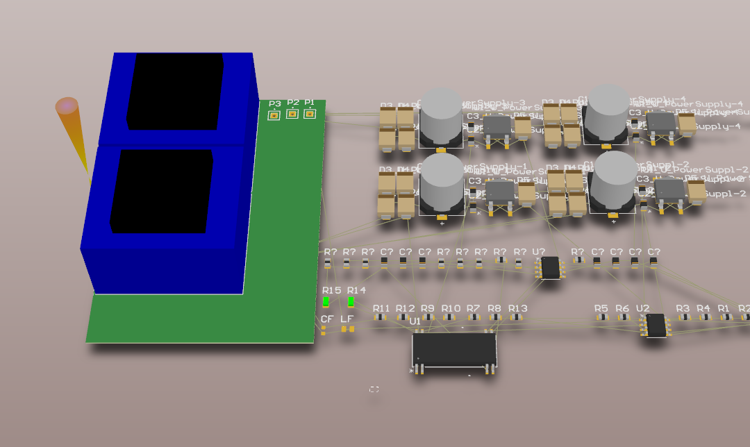 I'm finding it impossible to locate a small quad-secondary transformer, which would have a higher power density compared with two lower VA dual-secondary transformers. The OPA2134 op amp (I'm using two) and ISO124 chips all demand 2k ohm loads for ideal performance, which is before any output is actually connected. This is forcing up the size of the transformers and consuming space. I'll need to invest a lot of time into both reducing the sizes of components and thinking of clever placements if I'm going to fit everything in the box (which I certainly aim to).