Close
0%
0%

Mackerel 68k Linux Computer

A series of m68k computers designed to run Linux

Similar projects worth following
Mackerel 68k is a series of single-board computers based on the Motorola 68000. The goal of this project is to build a computer with each of the major processors in the family, from the 68008 through the 68040. Each iteration will add additional hardware peripherals, but the main software goal is to run Linux on every board.

Mackerel-08

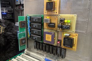
Based on the original prototype hardare, this SBC combines the 52-pin PLCC MC68008, a 512KB EEPROM, up to 3.5MB of SRAM, and a XR68C681 DUART on a single PCB. The DUART exposes two serial ports and three bit-banged SPI headers. One of these headers is currently used with an SD card breakout board to provide bulk storage to the system.

Mackerel-10

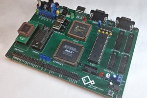
Mackerel-10 is the second phase of the project, It expands the design of Mackerel-08 with a 68010 CPU and 16-bit databus. Additionally, it increases the memory capacity with a DRAM controller implemented in a CPLD and up to 16 MB of 30-pin SIMM DRAM. An IDE header allows a hard drive or CF card to be connected as persistent storage.

Mackerel-30

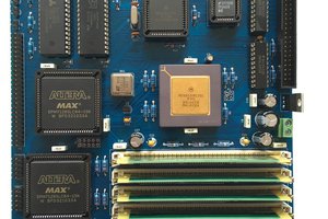
Based on the fully 32-bit 68030, Mackerel-30 adds a MC68882 floating point unit, 64 MB of 72-pin DRAM and support for modern Linux.

mackerel-10-v1.1.pdf

Mackerel-10 v1.1 schematic

Adobe Portable Document Format - 1.08 MB - 10/29/2024 at 16:42

Preview

mackerel-10-v1.1.gbr.zip

Mackerel-10 v1.1 Gerber files

Zip Archive - 754.16 kB - 10/29/2024 at 16:42

Download

mackerel-10-v1.1-bom.csv

Mackerel-10 v1.1 BOM

Comma-Separated Values - 2.84 kB - 10/29/2024 at 16:42

Download

mackerel-08-v1.1-updated.pdf

Mackerel-08 v1.1 schematic

Adobe Portable Document Format - 856.98 kB - 09/25/2024 at 00:52

Preview

mackerel-08-v1.1-BOM.csv

Mackerel-08 v1.1 Bill of Materials

Comma-Separated Values - 2.56 kB - 09/25/2024 at 00:49

Download

View all 6 files

  • 1 × Motorola MC68008FN10 PLCC-52 version of the 68008 CPU
  • 1 × SST39SF040 512 KB ROM 512 KB ROM
  • 7 × AS7C4096 512 KB SRAM 3.5MB total SRAM
  • 1 × XR68C681 Modern CMOS implementation of the classic 68681 DUART
  • 3 × ATF20V10C PLD Address decoding and glue logic

  • What's New For Mackerel-30?

    Colin M5 days ago 0 comments

    Rather than design a bare minimum prototype for Mackerel-30, I decided to take a bit more risk and incorporate most of features I want from the start. Moving from the 68008 to the 68010 was a reasonable step up in complexity. Jumping to the 68030 presents another significant leap with 32-bit buses and more complicated control logic. In some ways, it's actually easier to deal with though. The dynamic bus sizing removes the requirement for 16-bit ROM and RAM chips. A single 8-bit ROM and SRAM should be enough to bootstrap the system.

    Besides the new CPU, I've included a few other hardware upgrades. I'm looking forward to getting the MC68882 FPU up and running. It should be supported by Linux and might give a boost in performance for things like scripting languages or graphics support if and when I get to those.

    I've also upgraded to 72-pin SIMMs for the DRAM. Each SIMM is 32-bits wide which makes the wiring straightforward and requires only a single module. The available capacities are also quite a bit higher than 30-pin modules, going up to at least 128MB. The DRAM controller will be adapted from the one I designed for Mackerel-10.

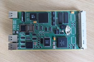
    The only piece I have not included in this first prototype is networking hardware. I'm still exploring some options in this area and I'm not ready to commit to one design. Once the base system is brought up, I plan to build a network card to connect to the expansion header.

  • Another Word On DRAM

    Colin M10/25/2024 at 04:15 0 comments

    Getting a DRAM controller working at all feels like a great accomplishment, and while it has been stable and functional, there were some situations I couldn't explain. For example, it was not possible to run the DRAM controller at anything other than twice the CPU speed, even running them at the same frequency failed completely. I was not satisfied with my understanding of my own design. I also wanted the option to run the DRAM on its own independent clock to completely free up the choice of oscillator for the CPU.

    With the goal of better understanding and more flexibility, I took the lessons learned from my first iteration and went back to the drawing board, starting with the datasheet. The simplest place to start is the CAS-before-RAS refresh.

    CAS-before-RAS Refresh

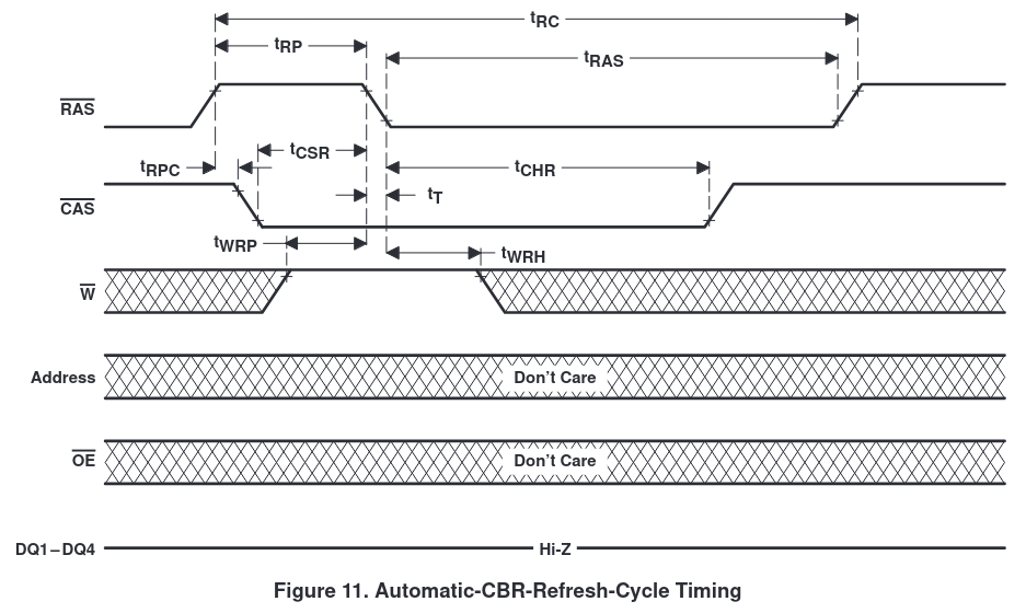
    CAS-before-RAS refresh timing diagram from the TMS417400 datasheet

    The refresh process is not complicated: pull CAS low, then pull RAS low, raise CAS, and then raise RAS again. One thing worth noting here is that the WE pin has to be HIGH by the time RAS is lowered. Since the state of the WE pin is "don't care" for the rest of the refresh cycle, I chose to pull it HIGH in the first state of the refresh state machine. Note: Mackerel-10 has four 30-pin SIMMs in two 16-bit pairs, A and B. RAS is shared between SIMMs in a pair, but the CAS lines are all independent, thus two RAS pins and four CAS pins in my controller.

    REFRESH1: begin
        // Acknowledge the refresh request
        refresh_ack <= 1'b1;
    
        // Lower CAS
        CASA0 <= 1'b0;
        CASA1 <= 1'b0;
        CASB0 <= 1'b0;
        CASB1 <= 1'b0;
        WRA <= 1'b1;
        WRB <= 1'b1;
        state <= REFRESH2;
    end
    
    REFRESH2: begin
        // Lower RAS
        RASA <= 1'b0;
        RASB <= 1'b0;
        state <= REFRESH3;
    end
    
    REFRESH3: begin
        // Raise CAS
        CASA0 <= 1'b1;
        CASA1 <= 1'b1;
        CASB0 <= 1'b1;
        CASB1 <= 1'b1;
        state <= REFRESH4;
    end
    
    REFRESH4: begin
        // Raise RAS
        RASA <= 1'b1;
        RASB <= 1'b1;
        state <= PRECHARGE;
    end

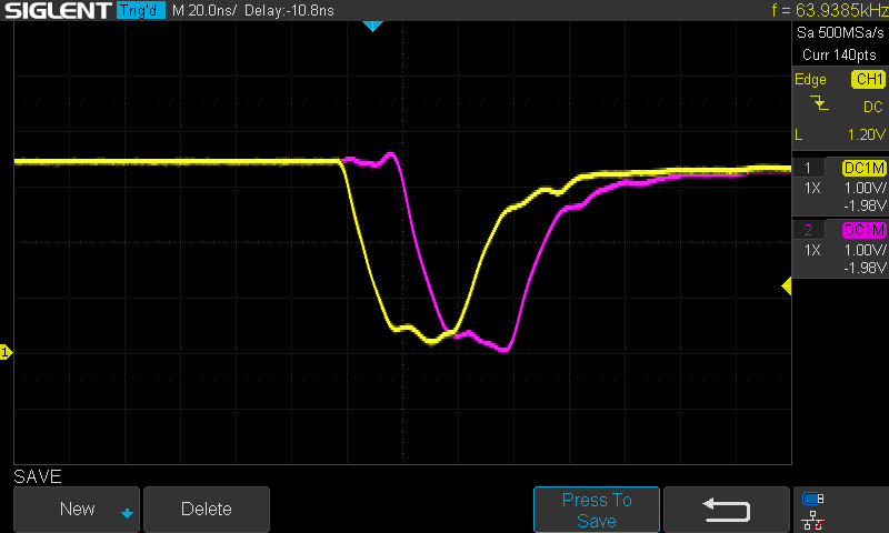
    The final piece of the DRAM refresh cycle is determining how often it needs to happen. According to the datasheet, all 2048 rows need to be refreshed every 32 ms. If we refresh each cell incrementally with CBR, that means we need to refresh a cell every 32 ms / 2048 = 0.015625 ms. That equates to 64 kHz. Finally, the DRAM controller is running from a 50 MHz oscillator, so 50 MHz / 64 kHz = 781 cycles between refreshes.

    The Verilog for counting cycles is basic, but I'll include it here for reference. The two refresh_ registers are used to pass the refresh state back and forth between this generator code and the main state machine. REFRESH_CYCLE_CNT is set to 781.

    // ==== Periodic refresh generator
    reg refresh_request = 1'b0;
    reg refresh_ack = 1'b0;
    reg [11:0] cycle_count = 12'b0;
    
    always @(posedge CLK_ALT) begin
        if (~RST) cycle_count <= 12'b0;
        else begin
            cycle_count <= cycle_count + 12'b1;
    
            if (cycle_count == REFRESH_CYCLE_CNT) begin
                refresh_request <= 1'b1;
                cycle_count <= 12'b0;
            end
            
            if (refresh_ack) refresh_request <= 1'b0;
        end
    end
    CAS-before-RAS refresh cycle running at 64 kHz as calculated

    Read/Write Cycles

    With the CBR refresh behavior confirmed, I started to revamp the rest of the state machine, i.e. the process of actually reading and writing memory. As mentioned, my first implementation worked, but just barely. One of the issues I had was a dozen or more compiler warnings in Quartus that looked something like this: Warning (163076): Macrocell buffer inserted after node. I could not track down an exact cause, but the little information I found online and my own testing seemed to indicate that this error basically means "you're trying to do much work at once". By breaking up my state machine into more smaller states and removing highly parallel pieces of code, I was able to get rid of all all these warnings. It seems like the key is not to change too many register values per clock cycle, but to instead pipeline the design.

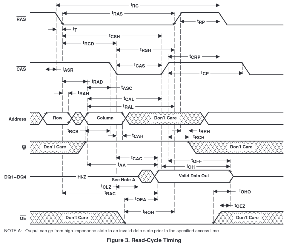
    DRAM read cycle timing diagram from the TMS417400 datasheet

    The actual logic of the DRAM read and write...

    Read more »

  • Linux IDE Driver And Hardware Updates

    Colin M10/20/2024 at 22:27 0 comments

    I've been making steady progress on Mackerel-10 since initial board bringup. The most exciting development is a working Linux driver for the IDE interface. There's now a real /dev/hda device accessible and this comes with all of the built in tools and filesystem support from the kernel. After adding fdisk and mkfs to the Linux image, the IDE drive can be partitioned and mounted as a persistent storage device right from Linux. This is a huge step in improving the usability of the system and it's a milestone for the project as a whole.

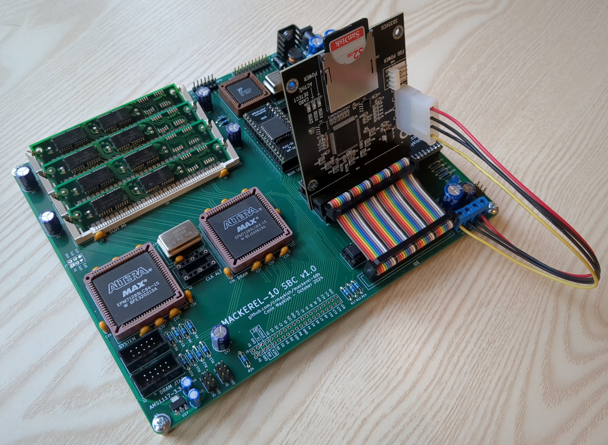
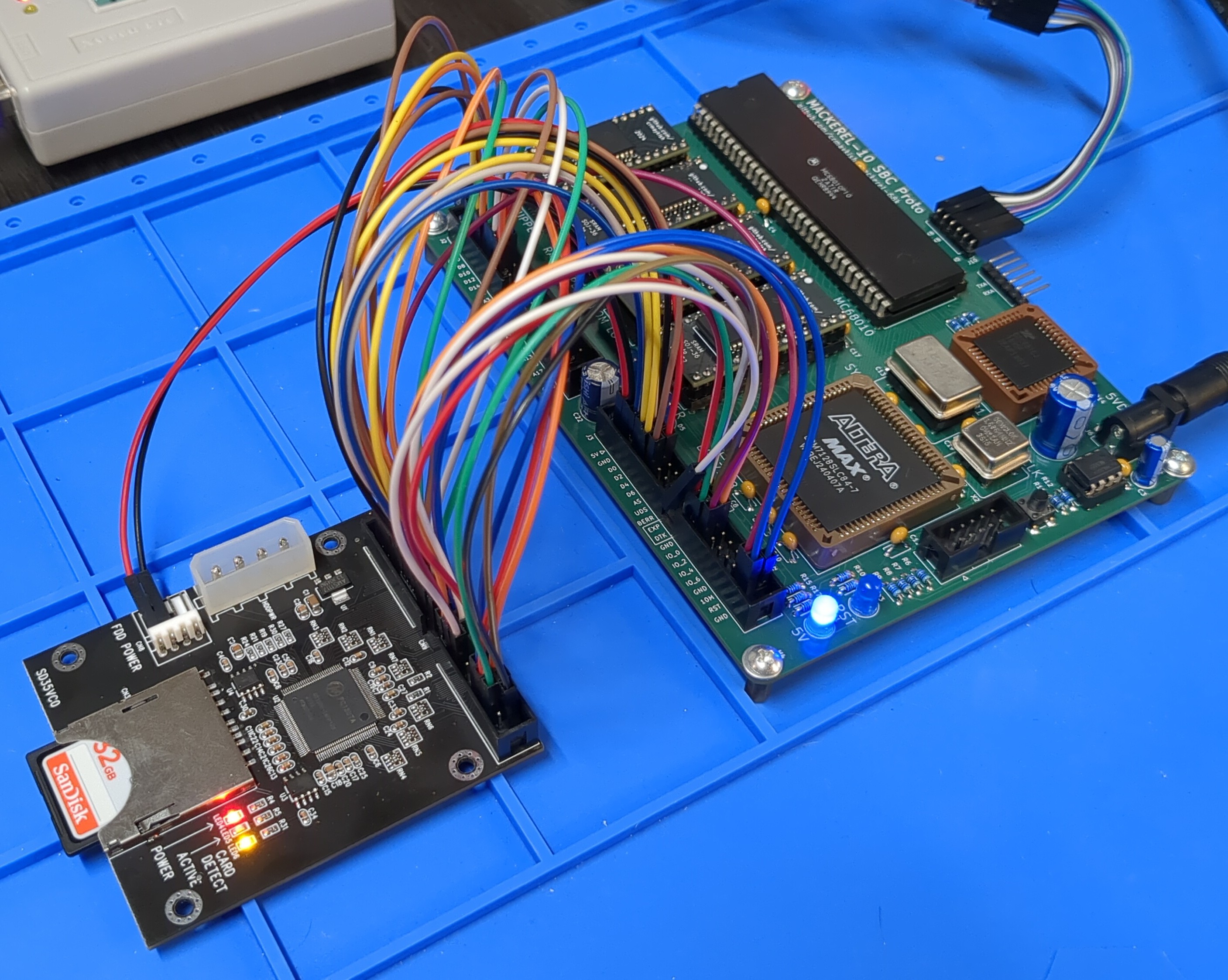
    Mackerel-10 with SD-to-IDE adapter

    Hardware Changes and Glue Logic

    The hardware design of the IDE interface was mostly complete before I started work on the driver, but there were a few updates to get everything fully supported. While it's possible to use IDE devices without interrupts, the Linux driver interface requires a working interrupt from the drive. This interrupt pin was already routed to the CPLD, so I updated the interrupt control Verilog to handle the extra source.

    The only sticking point on the wiring side was the missing second chip select line. IDE devices have two CS pins: CS0 and CS1. Only CS0 is required for basic functionality, but CS1 enables access to the alternate status register, a.k.a. the device control register. This register is needed to control interrupts on the drive. I did not have this pin connected to the CPLD, but it was connected to 5v through a pull-up, so I bodged a connection to one of the spare IO pins on the CPLD and updated the address decoding to make this device control register accessible to the CPU.

    Writing a Linux IDE Driver

    With the hardware and glue logic updated and tested in isolation, I started work on a Linux driver. There are a few different ways to implement IDE on Linux. The traditional (i.e. deprecated) way is to implement an ide_host and the associated functions for communicated with the drive(s). There's also a newer approach based on libata. This is a more modern solution, but it is not supported on m68k architecture, at least in the 4.4 kernel I'm running, so I implemented the traditional driver.

    Conceptually, the IDE driver interface is pretty simple. There are a handful of operations that the driver needs to define and the driver requires an interrupt number. On Mackerel-10, the IDE interrupt is autovectored to IRQ number 3. Implementing the required functions is fairly straightforward. For example, here are the commands that read the status, execute IDE commands, and read blocks of data:

    static u8 mackerel_ide_read_status(ide_hwif_t *hwif)
    {
        return MEM(MACKEREL_IDE_STATUS);
    }
    
    static void mackerel_ide_exec_command(ide_hwif_t *hwif, u8 cmd)
    {
        MEM(MACKEREL_IDE_COMMAND) = cmd;
    }
    
    static void mackerel_ide_input_data(ide_drive_t *drive, struct ide_cmd *cmd, void *buf, unsigned int len)
    {
        int i;
        int count = (len + 1) / 2;
        u16 *ptr = (u16 *)buf;
    
        for (i = 0; i < count; i++)
        {
            ptr[i] = MEM16(MACKEREL_IDE_DATA);
        }
    }

    The full driver code is available here: https://github.com/crmaykish/mackerel-uclinux-20160919/blob/master/linux/drivers/ide/mackerel-ide.c

    Dirty Hacks

    One issue remains with this driver. Normally, when an IDE interrupt is generated, the drive will assert the IRQ line and hold it until the CPU reads the status register. This clears the interrupt and normal operation resumes. For some reason, the interrupt on my system is never getting cleared. This means that after the first IDE interrupt, the driver just hangs and the system can't boot further.

    I managed to "solve" this by reading the status register manually in the process_int() function in ints.c if the vector number matches the IDE IRQ number, but this is a total hack. I don't know why the driver is not doing this automatically. It's entirely possible there's an issue with my interrupt glue logic or something dumb I missed in the driver code itself. I need to figure this out, but my hack is working for now and the IDE driver is fully functional.

    IDE drive partitioned...
    Read more »

  • Mackerel-10 v1: Lots of DRAM And A Hard Drive

    Colin M10/17/2024 at 16:54 0 comments

    The first round of PCBs for the Mackerel-10 SBC are in and I've begun assembly and board bringup. There aren't too many software changes going from the prototype to v1, but the hardware changed a little bit. There are now four 30-pin SIMM slots instead of two. These are arranged in two pairs to allow a 4x4MB DRAM configuration. Additionally, the IDE interface is now buffered through a set of 74HC245 chips to handle longer ribbon cables. The upper and lower bytes of the 16-bit IDE interface are also swapped in the layout to transparently convert the IDE little-endianness to the 68k's big-endianness. Finally, the pinouts of both CPLDs were completely changed to facilitate the routing of this board, so all of the pin mappings had to be updated in the Verilog projects.

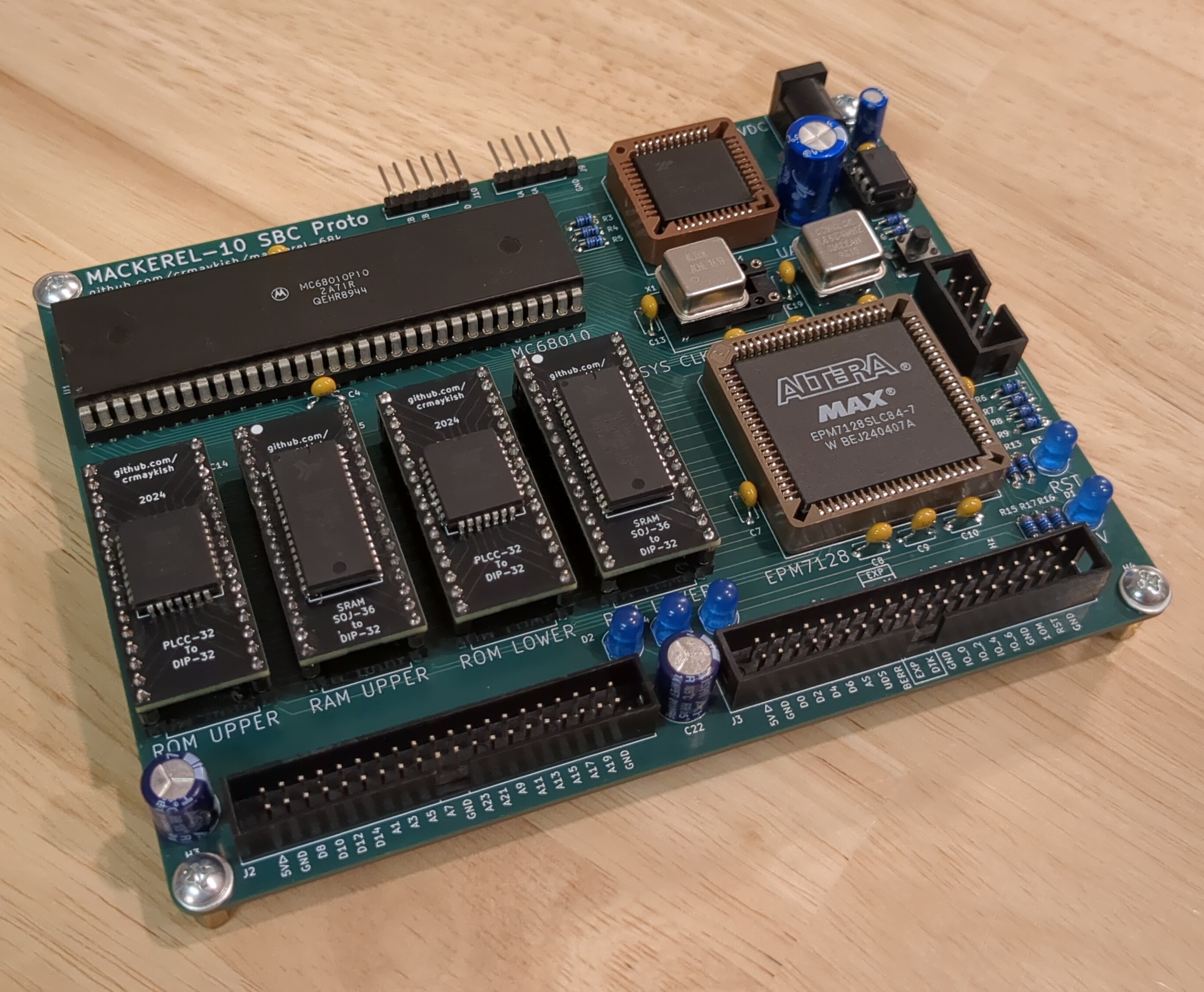
    Mackerel-10 SBC v1 assembled

    The core system (CPU, ROM, SRAM, DUART) came up pretty quickly once the glue logic and memory map was updated. The DRAM controller also works as expected. I had to update the DRAM controller to handle the extra two SIMM slots, but Mackerel-10 now has access to 14MB of DRAM. One megabyte is still used by the SRAM and the ROM and I/O share the remaining megabyte of address space. All in, that means we've now got 15MB of usable RAM on board.

    My DRAM controller is currently running fairly slowly (12.5MHz) at twice the CPU clock frequency (6.25 MHz). I added a second oscillator to the CPLDs with the hope of running the CPU and the DRAM controller on independent clocks, but I have not spent any time working on this. Ideally, the DRAM controller runs at whatever maximum frequency it can without having to worry about being in sync with the CPU clock. Since the DRAM bus access is asynchronous using its own DTACK signal, this should be possible, but I'll need to do some experimentaton and timing analysis.

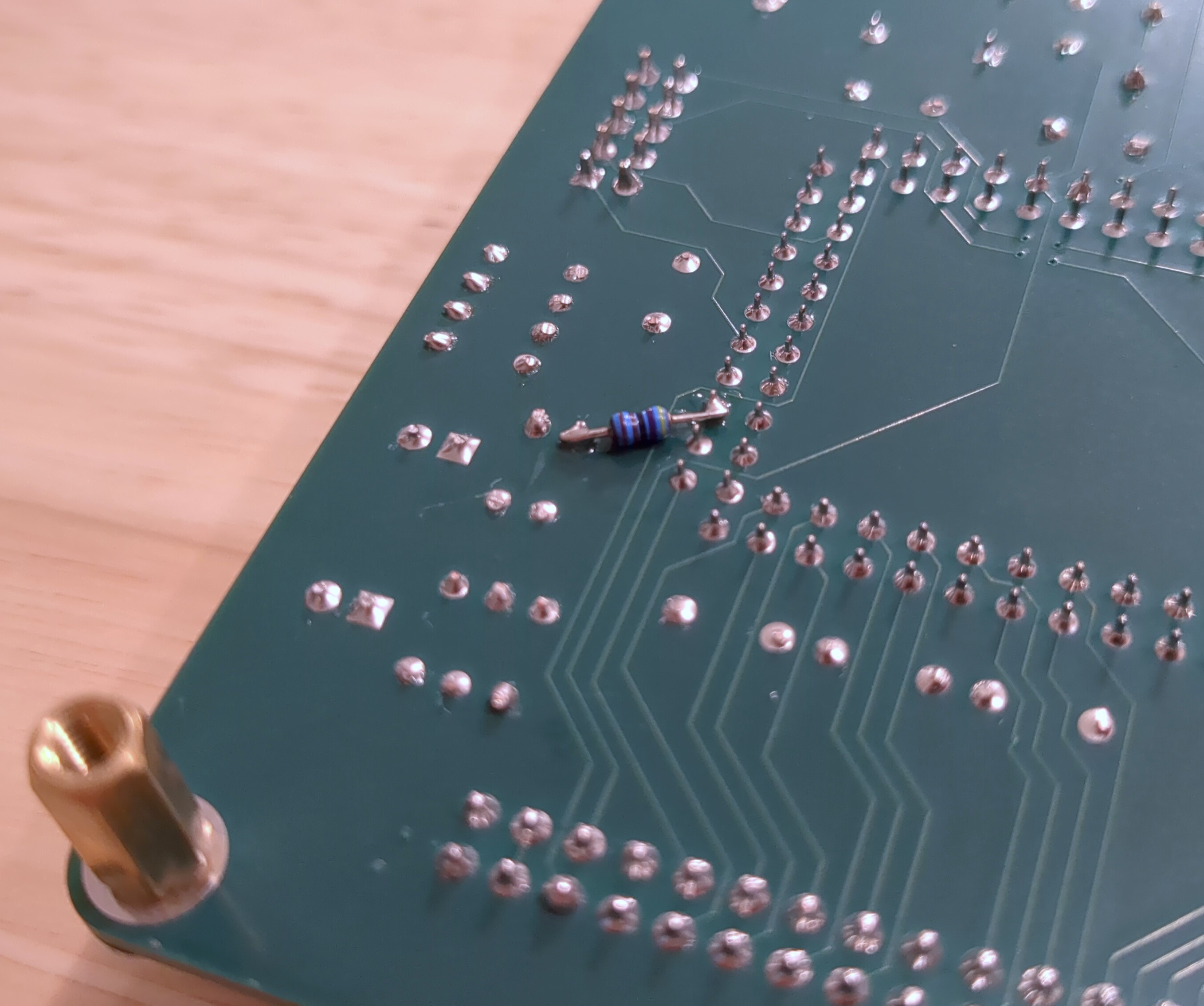
    The new IDE interface caused me some trouble. In the prototype, the 16-bit data bus from the CPU was wired directly to the IDE drive. Adding buffers between them will help with stability and lighten the load on the CPU data bus, but it adds a little more complexity and enough room to screw something up, which I did. After a lot of debugging with the oscilloscope, I realized the buffers are working fine, but the direction pin was inverted (or the A and B buses on the buffers were inverted, depending on your perspective). This meant the buffers were always pointing the wrong direction when the CPU tried to access the IDE registers. This was a dumb mistake I made in the schematic, but I was able to fix it by cutting the trace from the RW pin to the DIR pins on the buffers and creating the proper direction signal from one of the spare CPLD pins. With this bodge in place, IDE was functioning again.

    Bodge to fix the direction pin of the IDE buffers

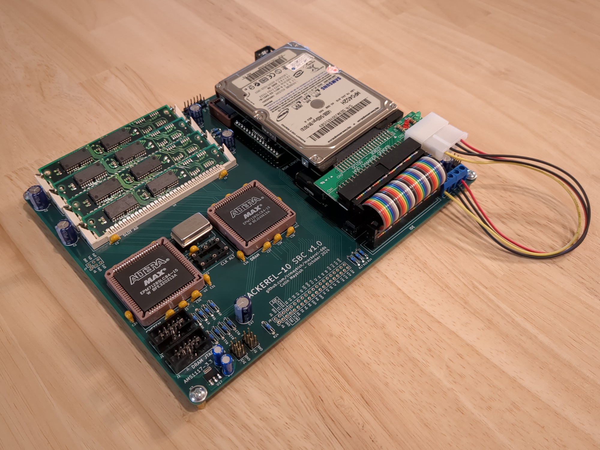
    There is minimal software support for IDE devices at the moment, but Mackerel-10 can read and write arbitrary sectors from the disk and print out drive identification info. I've done most of my testing with a SD-to-IDE adapter for simplicity, but I wanted to hook up a real IDE hard drive to make sure that was also working.

    Mackerel-10 with a real 2.5 inch IDE hard drive

    I'm a little disappointed about the IDE bodge, but I'm really pleased with the overall SBC. There are a few other minor issues with the v1 design that I will address in a future PCB revision, but my focus will now turn back to the uClinux port. I have a lot more RAM to play with and a real IDE device opens up a lot of options, at least once I figure out how to write a driver for it.

  • Mackerel-10 v1 PCB Design

    Colin M10/05/2024 at 23:09 0 comments

    In my last couple posts, I described the DRAM controller and IDE interface I've been working on. With both features working reliably, it's time to combine them together and build an SBC. One element I did not consider when making the jump from the 68008 to the 68010 is how much more complicated the actual PCB routing would be with all those extra pins. The DRAM controller also adds a lot of complexity to the routing and takes up a lot of board space.

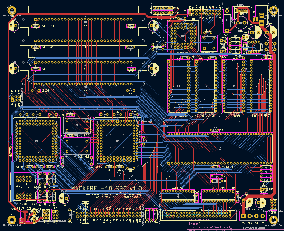
    I designed Mackerel-10 v1 as a four-layer board with the same stack-up as Mackerel-08, signal/ground/power/signal. The circuit design is not drastically different than the prototype PCBs I've been working with until now. The main difference is the on board IDE header and the addition of two extra SIMM slots. I wanted the option to use 4x4MB DRAM.

    I also broke out more I/O from the DUART and more power pins in general. I decided to keep the system expansion header limited to an 8-bit data bus with A1-A15 exposed, plus enough control signals to attach reasonable I/O devices. It did not feel necessary to expose the full 16-bit data bus or all of the address pins when most of the address space will be filled with on-board DRAM anyway.

    Finally, I added an optional second clock oscillator to both the system and DRAM CPLDs. I'd like to experiment with running the DRAM state machine on its own clock in an attempt to maximize both the CPU speed and the DRAM access efficiency.

    This is the biggest and most complex board I've routed so far. PCB manufacturing prices don't increase that substantially as the board size grows, so I did not go crazy trying to keep it as small as possible. It ended up being 210x170mm.

    Mackerel-10 v1 PCB signal layers
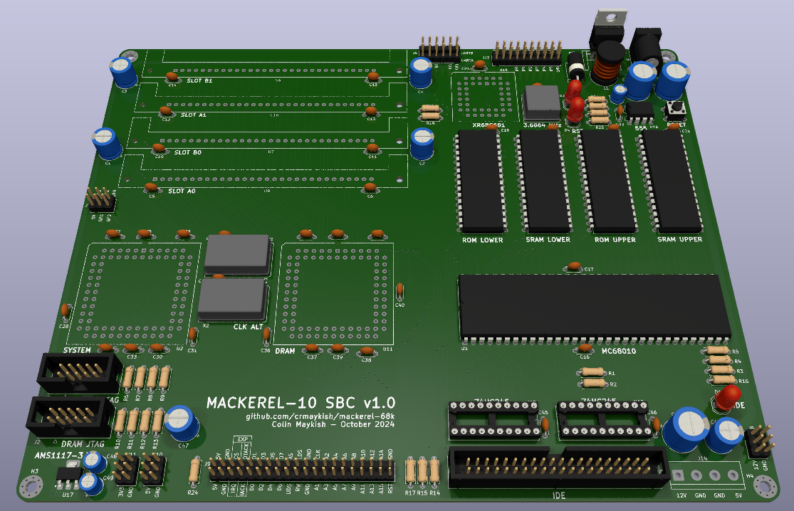
    Mackerel-10 v1 PCB render

  • Connecting an IDE Drive

    Colin M09/23/2024 at 02:57 0 comments

    With DRAM implemented, the next step for Mackerel-10 is to add support for IDE storage. Mackerel-08 has rudimentary persistent storage in the form of an SD card connected to the XR68C681's GPIO. The bitbang SPI protocol technically works, but it is incredibly slow. It takes about 4 minutes to load the 1.5MB kernel into RAM from the SD card. For Mackerel-10, I want something faster and more robust.

    IDE is actually somewhat of a natural choice for the 68000. Although the protocol has its roots in the x86 world, it's a fairly simple 16-bit memory-mapped register interface. It's possible to connect the full 16 data lines, 3 address lines, and a handful of control signals from an IDE drive directly to the 68000 with only a small amount of glue logic. I did just that.

    Mackerel-10 prototype wired to an SD-to-IDE board

    Ignoring interrupts and DMA for now, the only signals that don't map directly between the 68000 and the IDE interface are the chip selects and the read/write lines. IDE splits read and write into two pins instead of the single /RW pin of the 68000. I updated the glue logic in the CPLD to create the required signals and I put together some really basic C code to talk to the IDE device.

    The IDE protocol is actually really in depth, but for basic functionality, there's only a few pieces that matter. There are registers for data, status, error, and setting sector values and there's a command register with a list of supported commands. I've implemented two of these commands: DEVICE_IDENTIFY (0xEC) and READ_SECTOR (0x20).

    This is enough to read device info, e.g. model, firmware, and capacity details and to read arbitrary sectors of data from the drive. Sectors are transferred as 256x16 bit words. The only sticking point is that IDE, like x86, is little-endian and 68000 is big-endian so each word has to have the high and low bytes swapped. I've chosen to do this in code for now, but I've seen other projects implement this in hardware by simply wiring the data bus connection between the CPU and the IDE drive with the swap built in.

    It would have been nice to combine this IDE prototype and the DRAM breakout board to get a sense of what the full Mackerel-10 SBC will look like, but I did not think to design that option into the prototype PCBs. Oh well. I'm feeling good about this IDE test and my DRAM board has been very stable as well. I think it's time to jump back into KiCAD and start building the Mackerel-10 v1 PCB.

  • DRAM Controller and Verilog Simulation

    Colin M09/19/2024 at 23:36 0 comments

    Mackerel-10 now has a functioning DRAM controller and a serious boost to its total RAM in the form of two 4MB 30-pin SIMMs. With the 1MB of onboard SRAM, this brings the total usable memory to 9MB. Adding DRAM to any homebrew project always felt to me like a major milestone on the way to building a “real” computer. While it’s a long way from the complexity of modern DDR, it’s a significant step up in both complexity and capability compared to stacking a bunch of SRAM together (e.g. Mackerel-08).

    Mackerel-10 prototype with attached DRAM controller board

    I’m hardly the first person to add DRAM to a 68k system and I want to call out and thank a few projects I found to be terrific references while I was putting this together:

    - Lawrence Manning's MINI020 (and the rest of his 68k projects)
    - Tobias Rathje's T030
    - Stephen Moody's Y Ddraig

    All three projects implement some form of DRAM with a 68k CPU and I borrowed liberally from their implementations and write-ups. Thanks for sharing!

    The best decision I made while working on this was definitely taking the time to setup a Verilog testbench to simulate my implementation before trying to debug it on real hardware. In fact, I wrote the controller and simulator before I had any design for the hardware. Seeing the Verilog behave as I expected gave me a lot more confidence in my PCB design and saved a ton of time during board bringup.

    There are plenty of testbench tutorials out there and this is not one of them, but I used iverilog and GTKWave to simulate my design. Although I’m building and flashing the CPLD with Quartus (which includes ModelSim), I’d rather not spend a second longer than I have to in that program.

    There are two areas that make dynamic RAM more complicated to deal with than static RAM. The first issue is that the address pins on the SIMMs are not all exposed as they are on SRAM. Instead, they are multiplexed into rows and columns. This means that reading and writing data is no longer as simple as putting the full address on the bus. The basic read cycle for DRAM looks like this:

    1. Split the 24 bit address bus of the 68000 into row and column addresses (11 bits each in the case of 4 MB SIMMs)
    2. Write the row address to the SIMM’s address pins and assert the RAS (row address strobe) line
    3. Write the column address to the SIMM’s address pins and assert the CAS (column address strobe) line
    4. Read or write the resulting data

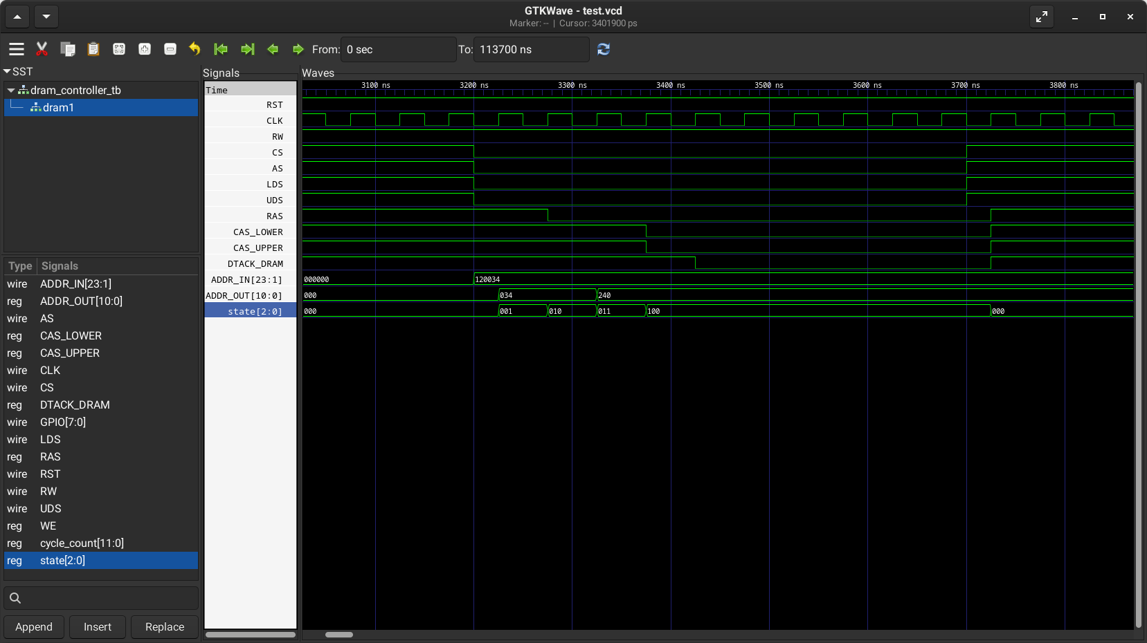
    Conceptually not too difficult to comprehend, but care has to be taken to meet the timing requirements at each one of these stages. My implementation handles this with a finite state machine. Each step in the DRAM cycle corresponds to one or more states in the FSM. Here’s what this read cycle looks like in simulation:

    Simulation of a 16-bit DRAM read cycle

    Once the DRAM responds with valid data, the controller will bring DTACK LOW and hold the data on the bus until the CPU brings the AS line HIGH, ending the memory cycle. This hold time is exaggerated in the simulation. A write cycle is almost identical except the WE pin on one or both SIMMs is asserted.

    The other challenge involved in using DRAM is the need to constantly refresh the memory cells. Every cell in the array has a maximum amount of time it can hold a value before decaying (DRAM is just a giant grid of capacitors). Refreshing a cell means reading it and immediately writing it back to restore the charge in the capacitors. Fortunately the DRAM chips provide a few ways to deal with this. The method I chose is CAS-before-RAS refresh. In a normal memory access cycle, RAS is asserted and then CAS is asserted. If the reverse is done, the DRAM will run a refresh instead. The DRAM chips are also kind enough to maintain internal addresses for the next refresh target, so all we have do is run a refresh cycle frequently enough to keep all of the cells topped off.

    Simulation of a single CAS-before-RAS refresh cycle

    Here you can see the relatively simple process of asserting...

    Read more »

  • Mackerel-10 is up and running!

    Colin M09/02/2024 at 01:01 1 comment

    Although the CPU, ROM, and RAM were simple enough to get running, I struggled quite a bit more with the DUART. I assumed it would be simple enough to port my glue logic and software from Mackerel-08, but there are a lot of moving parts in the 8-to-16-bit transition that all need to change at once. Testing just the hardware or just the software in isolation isn't really possible.

    The first hurdle was proving that the DUART was connected correctly and that it could be addressed at the appropriate memory addresses. I thought I was making my life easier when I set up some memory-mapped LEDs in the CPLD. Eventually this was extremely useful, but only after I remembered to add the RW pin to the decoding logic for it. This issue and my general inexperience with Verilog cost a few hours of debugging time, but eventually the serial port was screaming `AAA...`.

    Mackerel-10 first prototype fully assembled

    With a working serial port, my attention turned to software. I've already got a bootloader/monitor tool for Mackerel-08 that works well, so I started porting that to the new board. The two big changes going from the 68008 to the 68010 are a new memory map and the 16-bit wide ROM. The memory map is simple enough - just copy the .scr files from Mackerel-08 and modify the ROM and RAM locations to match up with the address decoding in the CPLD.

    Since each ROM chip is only 8-bits wide, but they are both addressed simultaneously by the CPU, the resulting binary code needs to be split in half. The simple way to do this is using `objcopy`. I updated the Makefile to do this:

    %-upper.bin: %.bin
    	$(OBJCOPY) --interleave=2 --byte=0 -I binary -O binary $< $@
    
    %-lower.bin: %.bin
    	$(OBJCOPY) --interleave=2 --byte=1 -I binary -O binary $< $@

    I found an example of this on Lawrence Manning's blog. He's built a few different 68k machines and I've learned a lot reading through his posts about them.

    While I was making changes to the Makefile, I added support to build all of the existing code for either Mackerel-08 or Mackerel-10. There are a few #ifdefs in the C code to handle the differences in hardware, but most of the heavy lifting is done by the Makefile itself.

    A working serial port and a working bootloader meant I no longer had to pull and flash two ROM chips for every code change. I could use the serial bootloader and load code directly into RAM. Note to self: ZIF sockets would have been worth the extra board size and cost on a first prototype. My fingers are sore from pulling the ROMs so many times.

    The final subsystem left to debug was interrupt handling. I ported the GAL logic from Mackerel-08 into Verilog for the CPLD and I set up all the pin mappings. Annoyingly, as soon as I enabled interrupts at all, the system would immediately receive one and jump to the unhandled user interrupt exception handler. After carefully checking the Verilog and C code, I realized that the DUART's IRQ output was always low (i.e. active). It turns out that I forgot to put a pullup on that line in Mackerel-10. Mackerel-08 has one and the datasheet specifies one as well. With the pullup in place, the vectored interrupts from the DUART were working just as they do on Mackerel-08.

    Bodged pullup on the DUART's IRQ output (connected on the CPLD side of the trace)

    With that small bodge in place, Mackerel-10 is fully tested. It functions just as well as Mackerel-08 minus some RAM and storage. The next step is to start implementing a DRAM controller!

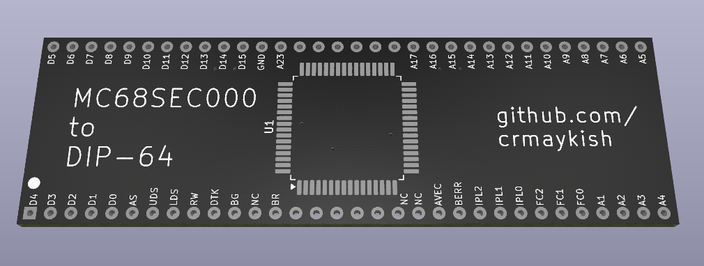
    Once I was happy that the 68010 was working, I had to push my luck and try this adapter for the MC68SEC000 that I made. It's designed to be a drop-in replacement for the DIP-64 processor. I assembled this adapter using the drag soldering method and plenty of liquid flux. I manually cleaned up a handful of bridges and scrubbed the excess flux away with alcohol then soap and water. I'm quite happy with the end results. I am even happier that it functions just fine slotted into Mackerel-10.

    Drop-in adapter board converts a MC68SEC000 CPU to a DIP-64...
    Read more »

  • Mackerel-10 Beginning Board Bringup

    Colin M08/30/2024 at 03:29 0 comments

    The next batch of PCBs have arrived. I spent an evening soldering and debugging the first prototype of Mackerel-10. I have only gotten as far as connecting the CPU, ROM, and RAM to the CPLD. The DUART is not working yet, but the 68010 is running C code that controls a memory-mapped LED register on the CPLD. No catastrophic design issues so far. Next step is to get the serial port working and modify some of the Mackerel-8 code to run on the new system. Without DRAM, I won't be able to run uClinux 4.4, but 2.0 should fit in the 1MB of onboard SRAM. I'd like to see that running on this hardware before I move ahead with a DRAM controller.

    Mackerel-10 in the middle of board bring-up

    In other news, Revision 1.1 of Mackerel-08 has also been assembled and mostly tested. It boots to a monitor prompt and passed my RAM test for all 3.5MB. I need to make a few small modifications to the code to support the new SPI layout, but things are looking good. Once SPI is working and I can stress test uClinux, I think Mackerel-08 is approaching hardware completion. I can continue to work on the software/Linux side, but it will be nice having a solid baseline going forward.

    Mackerel-08 Rev 1.1 assembled

  • Prototyping a 68010 Upgrade

    Colin M08/22/2024 at 19:30 0 comments

    The goal of the Mackerel project has always been to slowly work my way through the Motorola 68k CPU family, building new computers with each iteration. With Mackerel-08 fully operational, it's time to start thinking about its bigger brother, the 68000. Since building the same computer again with a faster CPU is not that interesting or enough of a challenge on its own, I'd like to add enough additional complexity with each new CPU to justify calling this a new computer.

    For Mackerel-10 that means three things:

    1. 68000/68010 CPU - either CPU should work in this system, but I will likely be using the 68010 for the relocatable vector table and the potentially higher clock speeds.

    2. DRAM - this is the big one. uClinux will definitely take advantage of more RAM and I plan to fill almost the entire 16MB address space of the 68010 with DRAM. I have a 4x4MB kit of 30-pin SIMMs and the appropriate sockets. I will be building a DRAM controller in an Altera EPM7128 CPLD to utilize it.

    3. IDE - Mackerel-08 has persistent storage in the form of a bit-banged SD card, but it is quite slow (somewhere around 3-5 kbps at best). I would like Mackerel-10 to have a full IDE interface for use with a real hard drive or a CF-to-IDE adapter.

    Although I just said building the same computer again is not the goal, that's basically what I've done here:

    Mackerel-10 mainboard first prototype design

    There are enough changes going from the 68008's 8 bit data bus to the 68010's full 16-bit bus and I've switched from using 22V10C GALs to a EPM7128 CPLD for glue logic, so I'd like to build this core system before adding DRAM and IDE hardware. This is also the first computer design I've done without building a hand-wired prototype or breadboard proof-of-concept first. Fingers crossed.

    This first PCB includes the 68010 CPU, 1MB each of ROM and SRAM, and the same XR68C681 DUART as Mackerel-8. If all of this works as expected, I will build a second board for the IDE and DRAM. This can connect back to the main system via the two 40 pin box headers. Once that second board is proven, I'll combine the designs back into one SBC, probably using the ITX form factor.

    As an additional little diversion, I've purchased some MC68SEC000 CPUs. They are rated to 20MHz, but I have read that many of them are stable at 50 MHz or higher. Sounds exciting! The SEC variant is basically a static version of the 68EC000 CPU, which is itself, a CMOS version of the 68000. I think it should be drop-in compatible with the original 68000 footprint provided there's an appropriate adapter. I was inspired by the Minimig project, but I couldn't find a source for their adapter, so I made my own:

    MC68SEC000 QFP-64 to DIP-64 adapter PCB

    I don't know if this will actually work, but it should be an interesting experiment. KiCAD project and Gerbers are available for this adapter on Github, but use at your own risk. This is still untested.

    https://github.com/crmaykish/adapters-and-breakout-boards/tree/main/MC68SEC000-to-DIP-64

View all 28 project logs

Enjoy this project?

Share

Discussions

tdurland wrote 10/28/2024 at 03:47 point

What speed are the 22v10c parts, on your BOM you left off the speed

  Are you sure? yes | no

Colin M wrote 11/07/2024 at 15:19 point

I'm using 15ns parts from Atmel.

  Are you sure? yes | no

tdurland wrote 2 days ago point

Could you post the jed files for the 3 gal chips and the hex file for the eprom

for the 68008 version 1.1

Thanks

  Are you sure? yes | no

Colin M wrote a day ago point

I've added the three JEDs and the bootloader binary here:
https://github.com/crmaykish/mackerel-68k/tree/master/releases/mackerel-08/v1.1

If you're putting together a board, send me a DM. I'd be interested to hear how it's going.

  Are you sure? yes | no

Daniel Palmer wrote 10/25/2024 at 13:44 point

I just stumbled across this project. Its possible to run a modern (as in Linus' master branch) kernel on 68000 as long as you have ~8MB of memory.

If you're interested I can point you to my repos with the changes needed and you could have a good getting it working on your board?

  Are you sure? yes | no

Colin M wrote 11/07/2024 at 15:16 point

Sure, I'd be happy to take a look. Building the latest kernel for m68knommu isn't too bad. I've gotten that far, but getting libc and a userspace all working was where I gave up.

  Are you sure? yes | no

Daniel Palmer wrote 7 days ago point

I have you covered on userland too. I have a recentish buildroot fork with enough patches to build a modern (ish, gcc 12 right now) toolchain and userland.

It's a bit broken for 68000 I think right now as I'm halfway through making 030, 040 and 060 work as well but I have buildroot, u-boot, linux and QEMU as a package here:

https://github.com/fifteenhex/m68kjunk

  Are you sure? yes | no

kanomi wrote 09/24/2024 at 22:20 point

In the schematic of  Mackerel-08-v1, I could not find any values of resistors (R1 to R20?).

In addition, those values were not printed on the PCB either. Can you tell me those resistor values?

  Are you sure? yes | no

Colin M wrote 09/24/2024 at 23:18 point

Sure, you've reminded me I need to clean up the schematic and post the BOM list. Until then, the resistor values are:
1k: R15, R20, R23
10k: R21, R22
4.7k: everything else

Also I realized that the PDF schematic I had on this project page was for v1. I've uploaded the v1.1 schematic. I'd recommend referencing that one. The resistor values and labels are the same on both, but v1.1 fixes some other issues.

Edit:
Here's the updated schematic with resistor values:
https://cdn.hackaday.io/files/1838617866309024/mackerel-08-v1.1-updated.pdf

  Are you sure? yes | no

Malcolm Harrow wrote 09/24/2024 at 13:25 point

Any early indications how much faster the IDE interface is compared to the SPI SD Card ?

  Are you sure? yes | no

Colin M wrote 09/24/2024 at 15:18 point

It's so much faster... On Mack-08, it takes 3m 46s to load the 1.2MB Linux image from the SD card. That works out to about 5.5 kB/s. On Mack-10, I was able to load 1024000 bytes in about 5.5 seconds - about 181 kB/s. That's a 32x speed increase.

Neither version of the code is well-optimized. I'm sure there are ways to improve the bitbang SD performance, but a 32x difference makes sense in a way. Mack-08 takes two memory cycles to read a single bit at a time (toggling the SPI clock up and down), whereas Mack-10 can read 16 bits in one memory cycle.

  Are you sure? yes | no

Malcolm Harrow wrote 09/22/2024 at 14:32 point

You may want to take a look here .. https://github.com/rosco-m68k/rosco_m68k/tree/develop/code/software/updateflash


there is some code to update the flash in situ if you write enable the chip (achieved on the board via a jumper).  Then you may not need the zif socket :)

  Are you sure? yes | no

Colin M wrote 09/22/2024 at 15:34 point

I considered implementing something like this early on in the project, but I never got to it. My issue was that once I could run code from ROM, I no longer needed to flash ROM very often - I'd just load new code over the serial port - so this just fell off the priorities list. Still a good reference though, thanks.

  Are you sure? yes | no

Malcolm Harrow wrote 09/22/2024 at 14:27 point

Very nice project.  I agree with you on Quartus, spend as little time as possible there!!   I have been trying to recompile the uClinux 4 source for the rosco_m68k board, but it’s complaining that it can’t find elf.h.  I’m working on a Mac and using the rosco cross compiler.   Could you let me know your setup to get a clean compile ?

  Are you sure? yes | no

Colin M wrote 09/22/2024 at 15:28 point

I'm not familiar with the compiler used by rosco, but Linux (and especially uClinux) is very picky about which compilers will actually build the kernel. You'll need a toolchain created specifically for it. Doing this natively on Mac is probably not going to work. You'll also need a x64 Linux machine or VM.

My setup looks like this:
1. Debian 12 (Ubuntu 22 or 24 should also work)

2. `apt install build-essential`

3. Download the uClinux 2016 toolchain: https://sourceforge.net/projects/uclinux/files/Tools/m68k-uclinux-20160822/m68k-uclinux-tools-20160822.tar.bz2/download
4. Extract that toolchain and make sure the `usr/local/bin/` folder is on your `$PATH`

5. From the root of the uClinux project, you should now be able to run `make menuconfig` and then `make`.

That's a pretty high level view. If you get this far though, you should be ready start porting uClinux to your rosco board.

If you get stuck, feel free to send me a PM. Happy to help.

  Are you sure? yes | no

Malcolm Harrow wrote 09/23/2024 at 00:10 point

Many thanks for the quick response .. I now have a compiling system !

I also had to apt install libncurses-dev to get the menu to work

There is also a newer version of the tools using gcc 12.3 .. its on the same account and called m68k-uclinux-tools-20231026.tar.xz

I will let you know I get on ..

Malcolm

  Are you sure? yes | no

Bharbour wrote 08/07/2024 at 02:44 point

Thats a good looking board!

  Are you sure? yes | no

Colin M wrote 08/07/2024 at 03:07 point

Thank you! There's always some minor things, but I'm really happy with how it came out.

  Are you sure? yes | no

teraz wrote 03/08/2022 at 19:53 point

Is possible make a mobile version? for example 24h working time?

  Are you sure? yes | no

Colin M wrote 03/09/2022 at 01:03 point

Sorry, not sure what you mean. Like a portable version of the computer?

  Are you sure? yes | no

teraz wrote 03/09/2022 at 10:44 point

yes, similar https://github.com/penk/penkesu , meybe solar panel too. motorola is power eficient

p.s. look this too https://hackaday.io/project/643-minibsd-laptop-computer 

  Are you sure? yes | no

Keith wrote 02/23/2022 at 22:34 point

I have designs for the 68008, 68000 and 68020. They all use SRAM so they would need hacking to exceed the 24 megabyte needed for an OS like Linux. My boards ran OS9/68K on a SCSI disk.
https://hackaday.io/project/28957-stebus-68008
https://hackaday.io/project/28960-stebus-68000 (board only, no cct or manual)
https://hackaday.io/project/28959-stebus-68020

  Are you sure? yes | no

Colin M wrote 02/24/2022 at 00:32 point

Nice looking boards. I like the idea of STEbus, but I'm not sure I'd want to invest a lot into it knowing I'll be expanding the bus width when I move up the 68k family tree. I guess most of the CPUs (other than the 68000) could actually use an 8-bit bus directly though.

I think I'm going to have to tackle DRAM when I need more than the 4MB that the 68008 can address. Buying and soldering all that SRAM sounds expensive and time-consuming.

  Are you sure? yes | no

Keith wrote 02/24/2022 at 00:44 point

The STEbus is 8-bit data but that does not stop processors being any data width they wish inside the board. For example, the 68020 board makes 16-bit accesses  to the ROM and 32-bit accesses to the RAM. The 68020 has "dynamic bus sizing", and will make accesses in whatever width the board logic tells it to. The STEbus is really just for i/o, not main memory. In the olden days, memory chip capacity was so small that extra boards were the only way to carry them. These days memory is big and cheap, and can easily fit on the processor board.

  Are you sure? yes | no

Colin M wrote 02/24/2022 at 00:55 point

Ah, that makes a lot more sense how you could get away with an 8-bit bus. I'm coming from a software background, so the system architecture, especially when it comes to things more complicated than SBCs, is definitely a learning opportunity for me.

  Are you sure? yes | no

bastetfurry wrote 02/23/2022 at 07:07 point

Regarding memory size, 24 MBytes seems to be the bare minimum these days for a recent kernel. How we found out? OpenComputers2 came around for Minecraft 1.18 and that one implements a RiscV64 VM with a barebone Linux on top. We tried to fire up a machine with just 16 MB inserted and got a genuine kernel panic as the userland refused to come up with just 4 MB of RAM left, the kernel alone eats up around 12 MByte. Inserted the 2*4 MByte from our very first try and voila, the machine came up to a login and we could run anything.

  Are you sure? yes | no

Colin M wrote 02/23/2022 at 15:03 point

This was on kernel v5?

I'll admit I've done very little research on what it will take to run Linux on this machine so far. Might have to stretch my definition of "modern Linux" a little to accommodate the 68008 limitations.

  Are you sure? yes | no

bastetfurry wrote 03/24/2022 at 09:51 point

Yep, made with recent buildroot, here is the fork: https://github.com/fnuecke/buildroot

  Are you sure? yes | no

Boxerbomb wrote 02/05/2022 at 19:11 point

Nice man, I will be following the project. I love 68k computers and I think that you are making the right choice trying to work your way up to the 30. I have been thinking about starting up a project like this and maybe using some sort of interface to a large RAM chip to avoid having to reprogram EEPROMS.

  Are you sure? yes | no

Colin M wrote 02/06/2022 at 04:46 point

Thanks, appreciate the interest. The build up from the 68008 is definitely less daunting than jumping straight into a 68030. My solution to constantly flashing ROM is a serial bootloader. I can load new programs into RAM over the serial port. The actual ROM code changes a lot less frequently that way. The only downside is you lose your program when you lose power.

I'm also working on a more direct boot-from-USB using the CH376S module. That will get its own write-up when I get it finished.

  Are you sure? yes | no

John Smith wrote 03/15/2023 at 18:16 point

Hi. Have you had a chance to complete the project and publish PCB gerbers for backplane and PLCC adapters?

  Are you sure? yes | no

Similar Projects

Does this project spark your interest?

Become a member to follow this project and never miss any updates