Close
0%
0%

CPU running Basic

Celebrating 50 years of Tiny Basic by implementing a custom micro-coded 16/32-bit CPU that executes it directly (up to 100MHz)

Similar projects worth following
TinyBasic interpreter Copyright 1976 Itty Bitty Computers, used by permission.

Can Basic be directly interpreted and executed by hardware? One of the recurring ideas in computing is one of "intermediate language" that provides abstraction over myriad differences between execution platforms. Pascal P-code, Microsoft IL (now known as CIL), Java VM bytecodes are some examples. 50 years ago, this concept was used to implement a minimal, portable Basic "dialect". Whole interpreter fit in 346 bytes of TBIL (Tiny Basic Intermediate Language) code! A VM ("virtual machine", another recurring concept) could then be written for popular microprocessors of the era, and for the first (and maybe last?) time same Basic code could be executed on vastly different computers. In this project I designed and implemented a custom micro-coded CPU that executes TBIL, within a "SBC" which also contains RAM, ROM, VGA and serial I/O.

See it running: https://www.youtube.com/watch?v=vVSzaxeds5I

Update 2026-04-15 - more performant interpreter approach and additional cache (8% perf gain), see project log entry. 

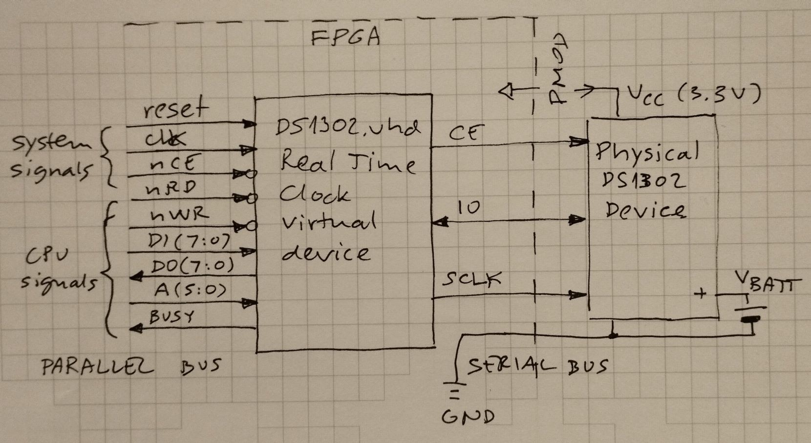
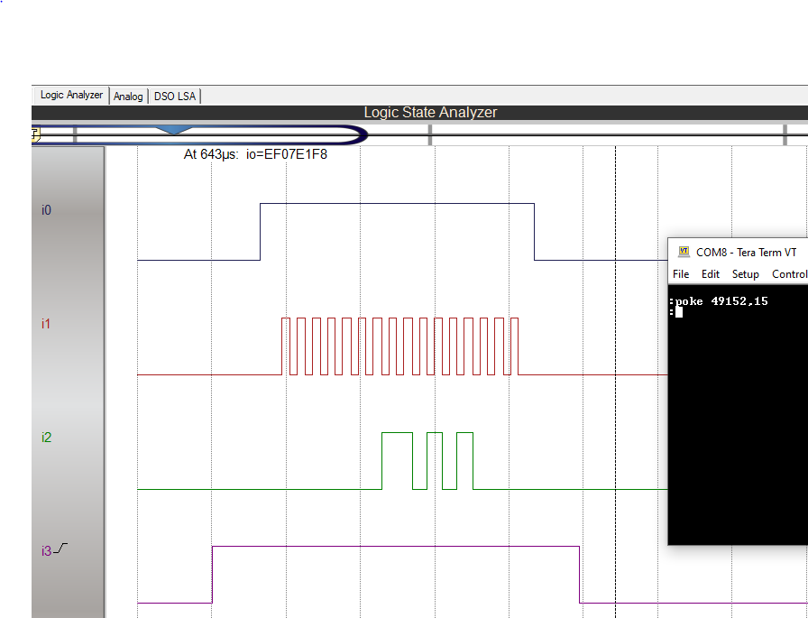
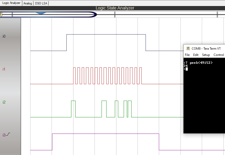
Update 2026-02-23 - Added Real Time Clock using DS1302 chip. See project log entry.

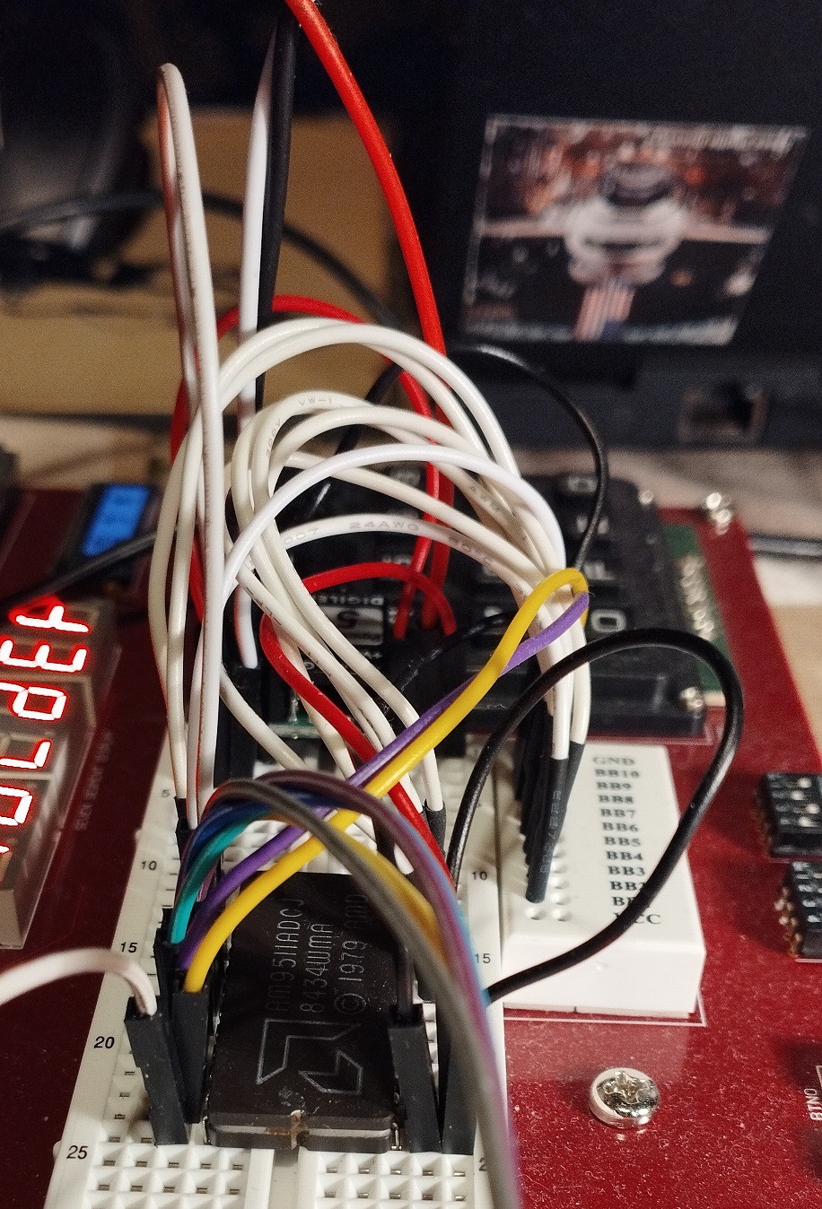
Update 2026-01-12 - Floating point support added using Am9511 co-processor. See project log entry.

Update 2025-12-11 - the Basic CPU now comes in 4 flavors: original and extended interpreter, 16 or 32 bit. Interpreter version can be changed during run-time, and word width during build-time, see project logs.

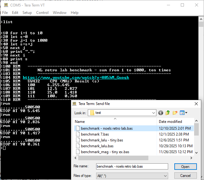
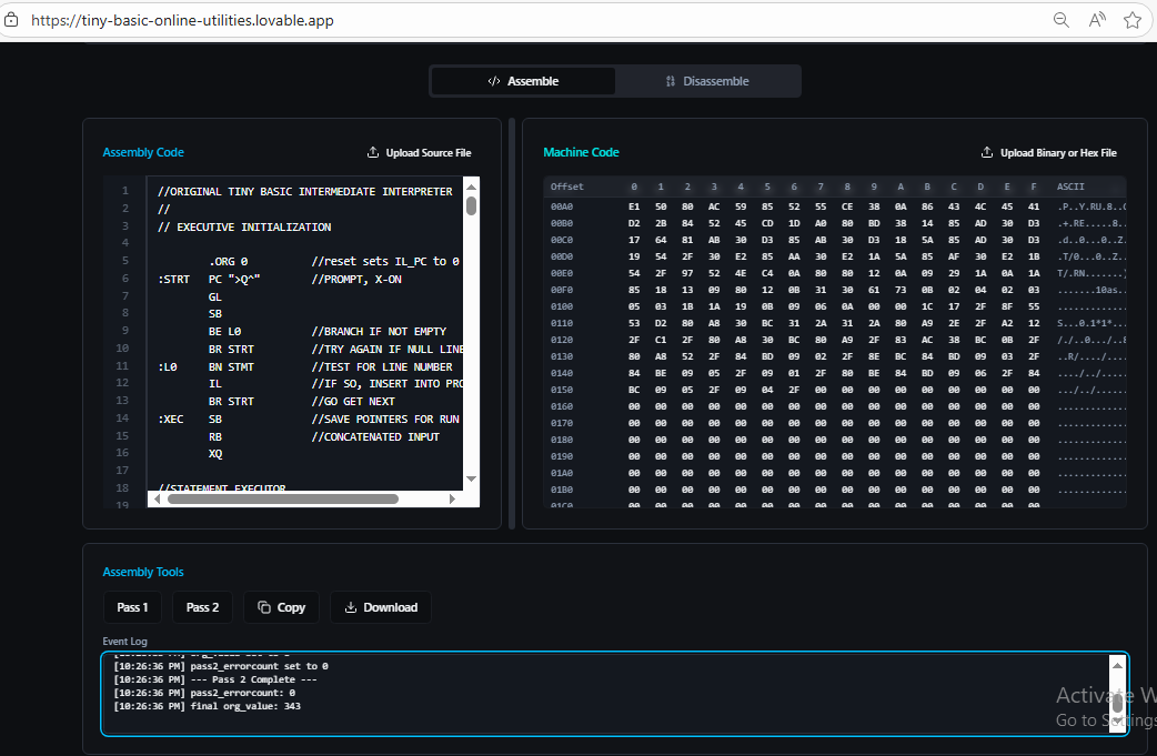
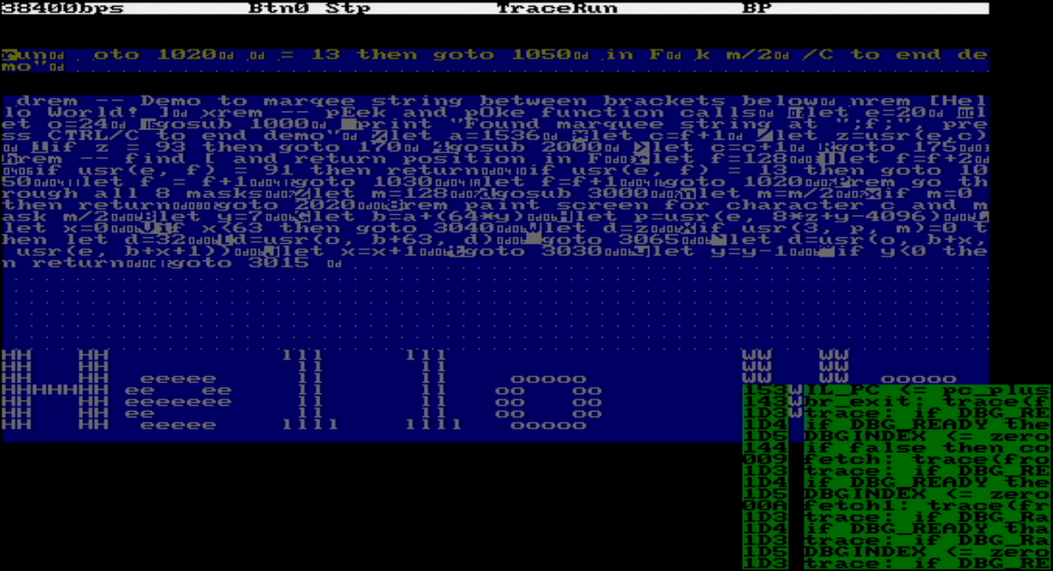
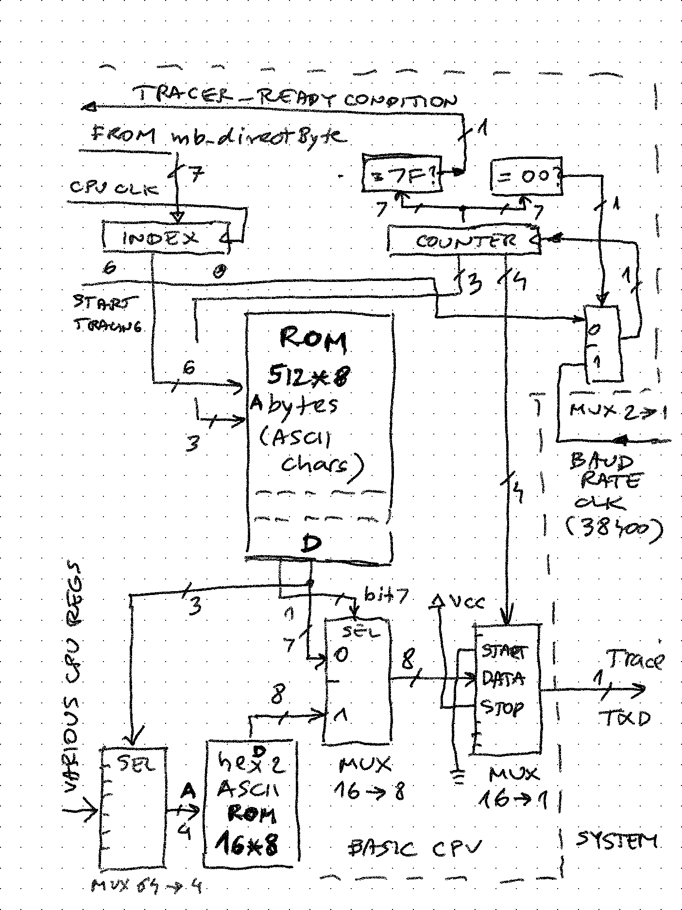
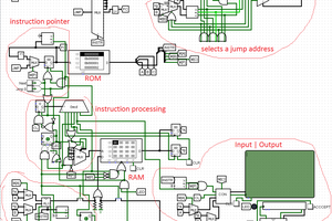
Homebrew CPUs are fun and fascinating - in implementations they span everything from relays to state of the art FPGAs, and in complexity and architecture they go from simplest one instruction machines to complex pipelined, superscalar processors. Where they often fail is going beyond demonstrating functionality. Writing any software for unique CPU requires much more time and different skills than designing and implementing an original CPU. This seems obvious, but  I re-learned the lesson on my own project too. As a result, few end up with even working monitor / assembler, not to mention some higher level programming language. What if we would reverse the order? Start with well known and accessible piece of software like Basic and build the CPU around it? The intermediary steps could then be used to replicate and make custom CPUs run some simple variant of Basic. Tiny Basic variant using intermediate / interpretive language (IL) - a programming masterpiece devised and implemented 50 years ago by folks in People's Computer Company - is especially suited to this because it is requires implementation of only about 40 operations / instructions in machine language of the homebrew CPU and voila - Basic will be running on it! In this project, this implementation has been done using a micro-coded machine extended with all the registers and stacks needed to execute those 40 instructions. Following the microcode, it is possible to see the implementation algorithm, as well as the power of micro-coding. Another secret goal was to see if I could maybe have the fastest running Basic ever :-) by tweaking the CPU implementation and microcode and measuring against an old benchmark.    

sys_microbasic_anvyl_32.bit

Binary for direct download (will work only on Digilent Anvyl board) - supports original and extended interpreters, 32-bit CPU

- 1.42 MB - 12/11/2025 at 02:14

Download

sys_microbasic_anvyl_16.bit

Binary for direct download (will work only on Digilent Anvyl board) - supports original and extended interpreters, 16-bit CPU

- 1.42 MB - 12/11/2025 at 02:14

Download

extended.tba

Extended interpreter from 2025 - can be assembled with https://tiny-basic-online-utilities.lovable.app/

tba - 7.09 kB - 11/27/2025 at 16:04

Download

original.tba

Original interpreter from 1976 - can be assembled with https://tiny-basic-online-utilities.lovable.app/

tba - 5.13 kB - 11/27/2025 at 16:01

Download

marquee_demo.bas

Displays "Hello world" (or any other text) as marquee on VGA (only works if the core memory is visualized through some display device)

bas - 1.08 kB - 11/17/2025 at 04:28

Download

View all 8 files

  • Speeding up the Tiny Basic interpreter

    zpekic04/01/2026 at 00:12 0 comments

    The original Tiny Basic interpreter relies on the BC (String match branch) instruction to do the parsing of keywords. After the 2-byte statement number (which is binary 16-bit value) the rest of Basic statement is a string, ending with CR (0x13). The "spec" for BC sounds a bit convoluted:

    BC a "xxx"   80xxxxXx-9FxxxxXx  String Match Branch.                                The ASCII character string in the IL
    following this opcode is compared to the string beginning with the
    current position of the BASIC pointer, ignoring blanks in the BASIC
    program. The comparison continues until either a mismatch is found,
    or an IL byte is reached with the most significant bit set to one.
    This is the last byte of the string in the IL, and it is compared as
    a 7-bit character; if equal, the BASIC pointer is positioned after
    the last matching character in the BASIC program and the IL program
    continues with the next instruction in sequence. Otherwise the BASIC
    pointer is not altered and the low five bits of the Branch opcode
    are added to the IL program counter to form the address of the next
    IL instruction. If the strings do not match and the branch offset is
    zero an error stop occurs.

    But seen in the code it is clear - compare with keyword, and if there is a match code to implement the statements continues after BC, otherwise jump to next BC which checks for next keyword:

     112 :RUN  BC CLER "RUN"
     113       J XEC
     114 .
     115 :CLER BC REM "CLEAR"
     116       MT
     117 .
     118 :REM  BC DFLT "REM"
     119       NX
     120 .
     121 :DFLT BV *            NO KEYWORD...
     122       BC * "="        TRY FOR LET
     123       J LET           IT'S A GOOD BET.

    At the end of the chain, assume the Basic statement was a <variable>=<expression> (assumed LET)

    While simple the problem is that the execution time grows with number of keywords implemented. Clever ordering of checks (e.g. PRINT or IF - very common, before CLEAR - which is rare) can speed up a bit but it remains a slow chain:

    100 LET x=100 ... executes "fast" because LET is first keyword to be checked

    100 x=100 executes much slower because x is recognized as a variable only after checking for LET, PRINT, IF, INPUT, POKE, GOTO, GOSUB, RETURN, REM, FOR, NEXT, CLEAR, NEW all failed.  

    Obviously, there is a much faster way - instead of n IFs, execute a single "switch" which checks the first alpha (A-Z) character in the Basic statement. If this is "x" we know right away it is implied LET because no statement starts with X. From the faster interpreter:

    //STATEMENT EXECUTOR
    :STMT    SA TRYQ        //switch on alpha char, or go to TRYQ label if not
        J LETLP        //a
        J LETLP        //b
        J C_BEG        //clear
        J LETLP        //d
        J E_BEG        //end
        J F_BEG        //for
        J G_BEG        //goto, gosub
        J LETLP        //h
        J I_BEG        //if, input
        J LETLP        //j
        J LETLP        //k
        J L_BEG        //let, list
        J LETLP        //m
        J N_BEG        //next, new
        J LETLP        //o
        J P_BEG        //print, poke, push, pop
        J LETLP        //q
        J R_BEG        //return
        J LETLP        //s
        J LETLP         //t
        J LETLP        //u
        J LETLP        //v
        J LETLP        //w
        J LETLP        //x
        J LETLP        //y
        J LETLP        //z
    
    :TRYQ    BC TRYARR, "?"        //? is short form of PRINT in many Basic dialects
        J P0            //yes, continue with PRINT statement
    :TRYARR J ARRAY
    •  If letter has no statement, go directly to implied LET
    • if letter has single statement, go directly to execution (e.g. RETURN)
    • if letter has multiple statements, execute a much shorter BC chain (e.g NEXT, NEW)
    • If no alpha letter, jump to default label. In case of Tiny Basic only 2 valid cases exist then: ? (abbreviation for PRINT, or @ to assign to element of built in array e.g. @(<index>) = <expression>

    SA is the new TBIL instruction (2 bytes, 0x28 <defaultcaseoffset>) implemented in microcode:

            ///////////////////////////* EXTENDED INSTRUCTION */////////////////////////////
            .map 0x28;                                    // SA (Switch on Alpha character)
            ////////////////////////////////////////////////////////////////////////////////
            traceString 4;                                // Trace mnemonic - TODO
            skipSpaces();
            MDR <= ToUpper, if...
    Read more »

  • Real Time Clock (using DS1302)

    zpekic02/23/2026 at 11:23 0 comments

    Real Time Clocks are probably one of the most useful devices any computer can have. Many FPGA boards are equipped with PMOD connectors, so it was convenient to use the module with already integrated backup battery and 32kHz crystal. 

    RTC module uses a very popular DS1302 chip, which contains in addition to clock also 32 bytes of non-volatile (battery backed up) RAM, handy for any value that should survive machine reset or loss of power. 

    CPU interfacing - parallel vs. serial

    Basic CPU is designed to use memory-mapped peripherals, which must appear as byte locations in the 64k CPU address space. The DS1302 IC is however serial. This means a component must exist that does the parallel to serial (write to RTC) and serial to parallel (read from RTC) conversions. 

    I wrote the DS1302.vhd, which works a bit differently than similar components I saw online. The CPU can access the RTC by reading/writing locations 0xC000 to 0xC03F (49152 to 49152+63 decimal)

    Writing to RTC RAM:

    1. BUSY output is asserted (i3 in screenshot below). This holds the CPU bus signals in frozen state. This is needed because CPU clock can be orders of magnitude faster than DS1302 clock (set to about 50kHz)
    2. 24-bit word is assembled which contains data, address, R/nW signals, as well as enable for DS1302, data directions etc. Data part is middle 16 bits, and 4 bits on each side 
    3. Control words are shifted on each falling edge of clk input
    4. SCLK (signal i1 below) is logical AND between input clk and internal enable
    5. control word are first 8 bits shifted out (signal i2 below) followed by data, LSB first. That's why 170 = 0xAA = 01010101 
    6. after 24 bits are shifted, BUSY signal is set to low, CPU can finish the memory write cycle and continue execution of the program
    Writing RTC RAM


    Reading from RTC RAM:

    1. all the steps as in write operation described above, except:
    2. there is internal "reg_dir" 24 bit control word. First 12 bits are low (IO pin on DS1302 is input) then high - which puts IO pin into tri-state ("Z" in VHDL) so data from DS1302 can be read
    3. DS1302 also outputs data byte LSB first, so 170 = 0xAA = 01010101

    Accessing clock registers - BCD to binary conversions and vice versa

    DS1302 registers 0 to 6 contain time/date values in BCD format. This means that setting clock to 23h one would have to write:

    POKE 49152+2, 2*16+3: REM writes 0x23 to hour register

    Of course, it is much easier for program to simply use:

    POKE 49152+2, 23: REM writes 0x23 to hour register

    Therefore, in addition to parallel / serial conversion described above, I also added binary to BCD conversion when writing to registers 0 to 6 and BCD to binary when reading from them. For both I use lookup tables (256*8 ROMs) defined here.

    Writing to seconds (BCD) register:

    Same as for memory write, but "bcd_reg" signal is evaluated and if "1" then data written to 24-bit "reg_io" register is passed through a "bin2bcd" lookup-table, otherwise goes directly.

    -- registers 0 to 6 are BCD encoded, so will do the conversion to binary for convenience
    reg_7 <= '1' when (A = "000111") else '0';
    bcd_reg <= (not reg_7) when (A(5 downto 3) = "000") else '0';
    dw <= bin2bcd(to_integer(unsigned(DI))) when (bcd_reg = '1') else DI;    -- binary to BCD when writing 
    

    Reading from seconds (BCD) register:

    Same as memory read, but if A input is in range 0..6 then data received is fed as address to a 256*8 lookup-table called "bcd2bin" which is defined in project common source definition file ("package" in VHDL parlance)

  • Floating Point using Am9511 coprocessor

    zpekic01/12/2026 at 19:42 0 comments

    TL/DR: Basic CPU can handle a rich set of floating point operations by interfacing with vintage AMD 9511 floating point co-processor. 

    "Serious" CPUs have co-processors, so why would Basic CPU be an exception? :-) Basic CPU supports only one data type: 16 or 32-bit signed 2's complement integer (there is also limited support for single bytes so some character operations can be implemented too). Most home computer Basic versions supported floating point numeric type, and often it was the default variable type. To implement FP in Basic CPU there were 3 options:

    ApproachProsCons
    Use FPGA vendor-specific implementations (for example, AMDAMD>State of art components, highly optimized
    >Working at full CPU speed (up to 100MHz)
    >"Black box" components limit learning value
    >not in vintage spirit
    >not "pure" VHDL, porting to other vendors requires changes

    Implement FP ALU and operations in VHDL/microcode>Transparent components - VDHL portable
    >fun learning how to implement floating point in hardware
    >Working at full CPU speed 
    >Microcode size would need to expand to control the new FPU component
    >FPU component would need to be also microcode driven, adding footprint and complexity
    Use external co-processor>Opportunity to play with fun vintage IC from the same Tiny Basic era>Speed bottleneck (external chip speed is limited, and much lower than CPU clock frequency)

    I went with option #3, using AMD Am9511 FPU. Beside familiarity with this IC, it is also easiest to interface with, as it is seen by CPU as 2 I/O or memory mapped 8-bit ports. It was specifically designed to be used by any 8-bit CPU, unlike Intel 8087 or NS 32081 which have very specific bus protocols and signals and are designed only to be paired with 8086 / NS 32xxx (of course, FPGA allows "spoofing" these co-processors too by replicating the other side of the signals / protocols)

    Hooking up Am9511 - hardware

    Anvyl FPGA board has a handy breadboard, so a messy but working prototyping is easy, with few constraints that must be observed:

    • FPGA board provides 3.3V, so USB-fed 5V PowerBrick provides this voltage
    • FPU also needs 12V, so a step-up voltage regulator (from 5V) provides it
    • Am9511 must be provided with CLK within a certain range (200kHz to 2MHz) which is much narrower than CPU (0 - 100MHz). The 2MHz limit is in a way OK, because the breadboard wire noise / impedance would not be able to support much higher anyways.
    • RESET signal must be of certain length for proper initialization, so I added a RESET delay circuit into the Basic CPU
    • Control and data bus work connecting directly to FPGA pins, which are nominally 3.3V.  

    Am9511 was designed to easily interface with many of the microprocessors of its era, with minimal "glue logic". That would be the case also with Basic CPU, but only if operating at the same clock frequency as the Am9511. That was clearly not acceptable so glue logic is needed to bridge the 2 clock domains: Am9511 works at fixed CLK of 1.5625MHz (100MHz/64), while the Basic CPU clock is essentially freely selectable from 0 to 100MHz. The solution is to drive the Basic CPU at FPU clock speed whenever CPU is accessing the FPU. However this CPU clock change must be done in controlled manner to avoid clock glitches that would cause the CPU to lock up. This interfacing (see schematic below) is implemented in the FPGA / VHDL, with only wires connecting to the breadboard. 

    All events in the Basic CPU happen at the low to high clock transition, which is important to the understanding of the clock generation and connections: 

    Sequence of events when Basic CPU initiates Am9511 read/write:

    1. Address 0xFFFX is presented on the ABUS. This pulls nSel_FFFX low (12-input NAND gate, actually implemented as 12-bit compare)
    2. A delay FF (flip-flop), driven by 100MHz clock (dark grey is 100MHz clock domain) drives signal nSel_FFFX_delayed. This means that there is a difference in value between selection and selection...
    Read more »

  • Same code, twice the width - 32-bit CPU

    zpekic12/11/2025 at 05:57 0 comments

    TL;DR

    I extended the CPU from 16 to 32 bits to specifically run the following benchmark, proposed by Noel's Retro Lab:

    I was most interested how 32-bit Basic CPU is performing relative to modern "retro" computers. They have fixed CPU clock, so I adjusted or interpolated results from runs seen above for comparison:

    System / CPUCPU clock (MHz)time (s) - quoted from hereBasic CPU time (s)relative performance
    ZX Spectrum Next / Z802851.273.94
    Agon Light / eZ80F9218.4321.81.051.71
    Mega 65 / GS451040.51.0470.881.19

    While these numbers favor the Basic CPU, in reality the systems above can run much more feature rich variants of Basic, with graphics, sounds, functions etc. while Basic CPU has only USR/PEEK/POKE at disposal. Still, not too bad for running an interpreter from 50 years ago on FPGA from 10 years ago. 

    Extending from 16 to 32 bits

    Most Basic variants support to 16-bit 2's complement integers. They are fine for many use cases, and arithmetic with them is reasonably fast even on 8-bit CPUs. Unfortunately, Tiny Basic has no Floating point support, so having just 16-bit integer can be limiting. So I decided to expand the CPU from 16 to 32-bits. The design goals were:

    1. No  changes to the interpreter - both original and extended interpreters can run on 16 and 32 versions
    2. Minimal changes to microcode - only where absolutely needed, for example 32-bit 2's complement integer convert to up to 10 decimal digits, while 16-bit to 6 so some loop counters etc. must be changed
    3. Changes to hardware are ok, but avoid any special case if/then if possible

    For #3, there were two possibilities:

    1. Run-time support for 16/32 bit switch. A bit like 65802 vs 65C02 - a flag or a pin flips the CPU to 32-bit mode. 
    2. Build-time support for 16/32 bit generation of the CPU itself. 

    I chose #2 as it seemed as easier implementation, and also because if I continue this project it is unlikely I would go back to 16 bit (next logical step is implementing Floating Point, which is viable only on 32-bit data / variables), and in that case all the complexities of supporting 16/32 will be present in the CPU, bloating the FPGA footprint and won't be needed right after boot into 32-bit mode.

    Parametric VHDL design

    The general idea here is to use feature of hardware description language to generate the registers and interconnections using parameters consumed during compile time. This code handles about 80% of what is needed to compile the design to be either 16 or 32 bit CPU:

    -- generics
    constant MSB_DOUBLE: positive := (MSB + 1) * 2 - 1;                            -- 31 / 63
    constant MSB_HALF: positive := (MSB + 1) / 2 - 1;                                -- 7 / 15
    constant ZERO: std_logic_vector(MSB downto 0) := (others => '0');            -- X"0000" / X"00000000"
    constant MINUS_ONE: std_logic_vector(MSB downto 0) := (others => '1');    -- X"FFFF" / X"FFFFFFFF"
    constant BITCNT: std_logic_vector(4 downto 0) := std_logic_vector(to_unsigned(MSB, 5));        -- 15 / 31
    alias IS_CPU32: std_logic is BITCNT(4);                                                                        -- '0' / '1'
    constant STEPCNT: std_logic_vector(7 downto 0) := std_logic_vector(to_unsigned(MSB + 1, 8)); -- X"10" / X"20"
    constant BCDDIGITS: positive := (MSB + 9) / 4;     -- 6 / 10
    constant CP_OFF: positive := MSB_HALF + 1;        -- 8 / 16
    type ram16xHalf is array (0 to 15) of std_logic_vector(MSB_HALF downto 0);
    type ram32xFull is array (0 to 31) of std_logic_vector(MSB downto 0);

    During build-time, parameter MSB is passed in as either 15 or 31, and then based on that various other values are determined, for example BITCNT which determines the number of steps during division, etc. 

    The above is not sufficient to create a functioning 32-bit CPU. The main problem is that the memory interface toward RAM that holds Basic code and input line remains 16 bit address / 8 bit data (64kb RAM), Basic line numbers are still meaningful only to 16 bits (due to the convention how Basic lines are stored) etc. The table below summarizes the major differences that had to be addressed with generating...

    Read more »

  • Extending Tiny Basic (to be more like another Tiny Basic)

    zpekic11/27/2025 at 00:04 0 comments

    While in it original form it can already be useful (esp. for embedded apps), the original Tiny Basic interpreter is very rudimentary and is lacking many features. During the same time, another Tiny Basic version emerged. It was a classic interpreter (no intermediary code) but had a bit bigger feature support. 

    With some minor tweaks, I was able to largely close the gap. What is missing:

    • Multiple statements on same line (there is limited support: only in run mode, and only after INPUT, LET, POKE, PUSH, POP statements. FOR/NEXT must be own statement, PRINT already uses ":", and for GOTO / GOSUB / RETURN makes little sense as they "jump" and not continue execution)
    • Logical operators in assignments
    • Specifying field length when printing values

    On the flip-side:

    • TB executed on Basic CPU is >5x faster than same Basic code on classic Tiny Basic interpreter on 8080 (35s vs. 197s both running at 25MHz)
    • Better handling of control codes (all ASCII control codes can be embedded in the print string using ^, including CR (^M))

    Here is the list of new capabilities and how they were implemented. Depending on the feature, changes were needed in any of the code layers (interpreter or microcode), or in hardware itself (Basic CPU)


    Basic feature
    InterpreterMicrocodeCPU
    NEWadded to parser and execute as CLEAR
    Note that neither CLEAR nor NEW clear the variables or Basic memory. A "POKE 129, 100" usually restores a program if there was one
    --
    FOR v=from TO end [STEP step]added to parser right after LET (for speed, more frequently used statements should be parsed out first). Interpreter just gets the variable name (must be A..Z, array elements not allowed), from and end value. If STEP is not given, default of 1 is pushed on stack and then then new instruction FS is executed.FS first checks if Vars_Next is populated. If yes, it means that this an iteration, therefore var = var + step, var > end must be executed. If no, means FOR must be set up with var = start, var > end. If FOR loop must be terminated, there are two cases:
    (1) pointer to NEXT exists, just go there and find first instruction after
    (2) pointer to NEXT is not set, so search for matching NEXT and then continue with case (1)
    Added CPU instruction 0x25 (FS) - there is a Vars_For field for each variable
    NEXT vadded to parser after FOR. Interpreter checks for presence of variable name A..Z (implicit NEXT with no variable name is not allowed) and then executes FE instruction.FE first ensures FOR has been executed for this variable (if not, that is clearly an error), and then puts the pointer in Basic text of this NEXT statement in the Next field. Branching back to FOR is easy because Vars_For contains the line number. Added CPU instruction 0x26 (FE), there is a Vars_Next field for each variable
    INPUT "prompt"Check for double quote before expression, and if found print out verbatim, then continue--
    multiple LET v=expr1, v=expr, v=expr...Modified LET to check for presence of comma after each variable assignment, and loop if present. --
    @(index) arrayAdded in LET command (left side) and expression evaluation (right side). This way it appears there is one array that can be used on both sides of expressions. New USR operations added:
    @(index) on left side (assign): USR(30, PrgEnd + 2* index, value)
    @(index) on right side (get value): USR(31, PrgEnd + 2* index)
    new operation in register T to evaluate address from index
    SIZE read-only variableadded parsing and evaluated as USR(29,...)SIZE = Core_End - PrgEnd. value of PrgEnd is evaluated at each warm start, which Core_End (last address in RAM) is currently hard coded. new operation on register T
    ABS() functionadded parsing and execute using already existing code path for RND()--
    % (modulo operator)added parsing and execute  through new USR(27, .., ..) call
    :T2    BC T3, "%"        //factors separated by modulo
        JS FACT
        LN 27            //a % b = USR(27, a, b)
        SX 1
        SX 5
        SX 1
        SX 4            //rearrange stack so that 0x001B (USR code) is at the bottom
     SX...
    Read more »

  • Vibe coding an assembler / disassembler

    zpekic11/23/2025 at 06:30 0 comments

    Note: the online utilities presented here are in progress, but the assembly part seems to be working, disassembler probably coming over the holidays, time permitting.

    My goal is to extend the Tiny Basic somewhat, to make it a bit more powerful and/or align it with other Basic dialects. For example, this could mean addition of:

    • FOR / NEXT loops
    • INPUT statement with prompt
    • multiple statements on a line (delimited by colon)
    • support for DATA / READ / RESTORE
    • parsing of integers in hex and/or binary format
    • possibly others...

    for all of the above - beside microcode changes - I also need to modify the interpreter itself, which is written in TBIL. To do that, obviously a TBIL assembler is needed. For this part of the project, to jump 50 years from 1976 (when Tiny Basic was introduced) to 2026 (almost there!) I decided to use some AI vibe coding. There are many such platforms, I am most familiar with Lovable. I created an online assembler / disassembler tool which allows TBIL source code to be assembled (2 pass) into binary / hex / vhdl file I could use to provide as code to the Basic CPU.

    Steps to try out the assembler:

    1. Navigate to online app
    2. Download the original version of interpreter
    3. Modify the interpreter, syntax is pretty obvious (only change from documented interpreter is that I use comma between branch target and "text" strings)
    4. Copy and/or upload the *.tba file using the "Upload source..." button
    5. Click Pass 1 button (observe if there are any errors)
    6. If no errors, click Pass 2 button (observe the action log)
    7. Binary code in hex format should appear in .... Switch to "Disassembly" mode to reveal the download options in .hex, .bin or .vhdl formats

    The source code of the app is here. All changes have been done by lovable dev bot, purely through "vibe coding". I did a similar vibe coding online tool about 6 months ago and I see certain improvements. At that time, often after changes there would be a build break. When I developed this new app, there was no build break at all. 

    Vibe coding is still just .. coding

    What this means is that all the good coding advices still apply. Most notably, everything about planning and designing the app before writing the actual code. In this case the UX of the app is rather boilerplate, using a one-page layout with standard controls such as editable text boxes, file upload / download, resizable panels, buttons etc. The AI tool shines with this part (although the code it produces is still bloated and slow, requires targeted prompting to refactor it into a leaner implementation), but where it obviously needs serious prompting is the business logic. After all, there is no proliferation of TBIL assemblers from 40+ years ago it can learn from :-) I put effort to explain exactly what needs to be done for each line of source code in both pass1 and pass2 of the assembler. I also included some links for context. Therefore, when I asked it to implement assembly pass 1 and 2 it was "on rails" and fairly successful, with only minor tweaks needed. 

    The original text of the instructions I provided ("knowledge" in Lovable parlance) is below. I also asked it to extract it as markdown document file and check it in. I organized the "knowledge" into:

    • Links for more context (targeted sources as generic "Tiny Basic" would completely confuse it)
    • Concepts. Each concept is as clearly defined as possible and includes "action" when applicable (what to do when concept is encountered)
    • Steps for pass 1, organized by assembly instruction
    • Steps for pass 2, organized by assembly instruction
    http://www.ittybittycomputers.com/IttyBitty/TinyBasic/TBEK.txt
    https://hackaday.io/project/204482-celebrating-50-years-of-tiny-basic
    http://www.ittybittycomputers.com/IttyBitty/TinyBasic/
    
    DEFINITIONS USED FOR ASSEMBLY PASS1 AND PASS2:
    octaldigit
    
    octaldigit is single digit in range 0 to 7 (inclusive). Represents values 0 to 7
    
    constant
    
    constant is...
    Read more »

  • "Hello World!" demo

    zpekic11/18/2025 at 18:38 0 comments

    What would a CPU project be without a "Hello World" demo? :-)

    I originally introduced VGA display as a debugging tool to visualize content of Basic input line and program (esp. GL and IL instructions), as described here. But once display surface exists, why not use it as simple text-based screen output? 

    Tiny Basic system currently implements 2k RAM mapped to address space 0x0000 to 0x07FF. If the program is shorter than that, whatever remains can be used as "window" for example 8*64 in size, starting at RAM location 0x0600 or 1536 decimal.

    For the demo to work, 2 additional capabilities were needed:

    • Ability to access Basic RAM (classic PEEK and POKE)
    • Ability to read the font definition for the characters in the scroll, and "magnify" them by 8X so that 8*8 pixel becomes 8*8 character.

    Memory mapping

    Total Basic memory space is 64k, leaving 62k open in the system. I used the top 4k to access same character generator ROM VGA controller uses (two copies of this ROM are now in the design). This char gen has 8*8 font similar to C64, but I also added representation of control characters 0x00-0x1F which help with debugging (note CR in memory display above after each Basic statement). From the outside, the char gen appears to hold 256 characters, but the capacity is only 1k, ASCII codes 0x80..0xFF are inverse duplicates of 0x00..0x7F.

    sel_hi4k <= '1' when (A(15 downto 12) = X"F") else '0';
    memData <= pattern when (sel_hi4k = '1') else ram(to_integer(unsigned(A(10 downto 0))));
    D <= memData when ((nBUSACK or nRD) = '0') else "ZZZZZZZZ";
    
    -- Character generator ROM handy for the marquee demo
    chargen: entity work.chargen_rom port map 
    (
        a => A(10 downto 0),    -- 256 chars (128 duplicated, upper 128 reversed) * 8 bytes per char
        pattern => pattern
    );

    USR() function

    The original Tiny Basic ran on a number of microprocessors from 1970ies/80ies. To allow extensibility, each implementation of TBIL interpreter was supposed to define and implement the r = USR(a, p1, p2) call from Tiny Basic, where:

    • a - address of the native (assembler / machine code) routine to call
    • p1 - required parameter 
    • p2 - optional parameter
    • r - result

    All of the above were 16-bit values. For example:

    argument \ CPU  650268001802
    aJSR aJSR aR3=a, P=3, X=2
    p1MSB=X, LSB=Y (to be verified!)X (16-bit)R8
    p2AARA
    rMSB=A, LSB=Y, RTS to returnA, RTS to returnMSB=RA.1, LSB=D, SEP 5 to return

    At minimum, implementing PEEK / POKE was expected, but any other (such as direct reading of keyboard etc.) was possible. Only option for Basic CPU was to implement in microcode some of the most useful USR calls, and these are also used in the Scroll demo Basic program

    Currently implemented: 

    Functionap1p2rused in demo?
    Logical0 .. 716-bit word16-bit wordp1 op p2a = 3, which is logic AND operation
    PEEK820address of byte to updateN/AM[a]yes
    PEEK1621address of word (on any byte boundary)N/A256*M[a]+M[a+1]no
    POKE824address of byte8-bit value to write to memory addressed by a (upper 8-bit of the value is ignored)p2yes
    POKE1625address of word (on any byte boundary)16-bit value to be written to a in big endian representationp2no

    To save on the "switch" statement that would take precious microcode, all binary logic operations are implemented with the same expression, controlled by 3 lowest bits of parameter a. 

    (omitted)            
    when T_binop =>
        -- S    operation
        -- 0    T NOR R
        -- 1    T NOR /R
        -- 2     /T NOR R
        -- 3    T AND R
        -- 4    T OR S
        -- 5    T OR /S
        -- 6    /T OR S
        -- 7    T NAND R                
        T <= S2 xor ((S1 xor T) nor (S0 xor R));
    (omitted)
        
    -- masks for T_binop
    S0 <= (others => S(0));
    S1 <= (others => S(1));
    S2 <= (others => S(2));

  • Chasing performance

    zpekic11/17/2025 at 06:21 0 comments

    I was really curious how the Basic CPU will perform in comparison with classic CPUs of the home computer era and put some effort into optimizing the design with that goal in mind. Based on the benchmark tests, the goal has been only partially achieved. While in some cases the speed up of factor 4 to 8 looks noteworthy, my suspicion is that those Basic interpreters by default work with software - implemented floating point for the benchmark test (haven't explored them in depth), while other group showing more modest gain of 1.5 to 2X are "integer Basic" implementations, and a more fair comparison. 

    CPU performance optimizations I used:

    Clock frequency

    A bit of "cheating" going on here - whole design is inside the FPGA which allows it to work at maximum available hardware clock frequency of 100MHz. Most importantly, the "core" RAM (Basic input buffer and program store) can be accessed in 1 or 2 clock cycles (so 10 or 20ns):

    writeCore:    nWR = 0, if nBUSACK then repeat else return;
    
    readCore:    nRD = 0, if nBUSACK then repeat else next;
            nRD = 0, MDR <= from_Bus, back;

    This would clearly be impossible if the RAM is outside of the FPGA, even on the same board.  Depending on the CPU clock and memory speed, one or more wait cycles would need to be added. Anvyl board has a breadboard section, so in future I may move the Basic core memory to a 62256 type device and experiment for example how many wait cycles does a 70ns vs. 120ns memory chip need. 

    Other limiting factor is I/O speed. Currently, max I/O serial speed is 38400 bps. Sending and receiving 1 byte over such channels takes at least 10-bit times, during which CPU has to wait for the ready signal. 

    outChar:    if CHAROUT_READY then next else repeat;            // sync with baudrate clock
            if CHAROUT_READY then return else repeat;

     FIFO queue on both input and output would help, but their implementation belongs to the Ser2Par and Par2Ser components, not the CPU (except for the trace serial output, but that one is only active up to 4kHz CPU frequency so not much gained there). 

    Cycle overlap

    Basic CPU is a CISC processor, and pipelining is not traditionally their strength. However a very limited opportunity of overlap is used between execute and fetch in few instructions. Note that the fetch cycle has two entry points:

    fetch:        traceString 51;                        // CR, LF, then trace Basic line number (in hex, for speed)
    fetch1:        traceString 2;                             // trace IL_PC and future opcode
            IL_OP <= from_interpreter, IL_PC <= inc, traceSDepth;    // load opcode, advance IL_PC, indent by stack depth IL code if tracing is on
            T <= zero, alu <= reset0, if IL_A_VALID then fork else INTERNAL_ERR;    // jump to entry point implementing the opcode (or break if we went into the weeds) 

    Most instructions finish their execute cycle and then branch back to "fetch" (no overlap). Few have the opportunity to execute "traceString 51" operation while in parallel doing other operations, and when done can branch to "fetch1" - this is a 1 clock cycle overlap. This could be utilized more, but tracing at the beginning of fetch cycle is very convenient debug tool, so this was an engineering compromise between 2 important goals (troubleshooting and performance).

    ////////////////////////////////////////////////////////////////////////////////
    .map 0x12;                    // FV (Fetch Variable)
    ////////////////////////////////////////////////////////////////////////////////
    traceString 36;                    // trace mnemonic
    Vars <= indexFromExpStack, if STACK_IS_EMPTY then ESTACK_ERR;     // get index (variable name A-Z)
    T <= from_vars, ExpStack <= pop1, traceString 51;        // T <= Vars(index)
    ExpStack <= push_TWord, goto fetch1;                // push onto stack, go to 2rd fetch entry point as we overlapped 1 cycle

    Parallel operations

    Basic CPU uses "horizontal microcode" with fairly wide control word of 80 bits:

    • Microprogram execution control: 5 bits to select 32 conditions, 9 bits to...
    Read more »

  • Debugging

    zpekic11/14/2025 at 02:46 0 comments

    Complex programmable logic designs are opaque. Unless this opaqueness is turned into transparency, the design and the whole project will fail. I use mainly two methods to peek into the (quite literally) little black box of FPGA:

    • Create generic components and test them in separately or inherit them from projects in which their already worked. Examples in this project that I reused (with some modifications):
    • Build into the project itself as many as possible debug features, starting with simpler (LEDs, buttons) towards more complex (serial debug, VGA) as the project progresses
    component \ visualizationLEDs, 7-seg LEDsSerial outputVGA
    serial to parallel inputLEDsEcho of input buffer during GLInput buffer hardware window
    CPU register TtraceT(); microcode subroutineDisplayed using block cursor at the locations it points to
    CPU registers BP, LS, LE, PrgEnd7-seg LEDstraceBP(); Underline cursor shown at location pointed by register
    ALU registers-traceALU(); -
    CPU return stack-displayed as indentation of each IL operation-
    Microcode execution(program counter can be displayed)-Hardware window, using symbols from symbols ROM produced by microcode compiler
    IL execution-Each IL instruction traced with mnemonic and parameters -
    Command line--Hardware window
    Basic program--Hardware window
    GOTO cacheOnly empty/used/full state on LEDs--

    Armed with the above, I was able to visualize and debug the 3 layers of code:

    1. Microcode executes TBIL instructions
    2. TBIL instructions execute Basic interpreter
    3. Basic interpreter executes user's Basic program

    Two components important for debugging merit some discussion as they are useful and generic enough for other programmable logic projects too:

    Serial Tracer

    Basic CPU has an output - only serial port which outputs a constant stream of trace data, whenever microcode includes a call to the "traceString nn" subroutine. nn is a number from 0 to 63 (can be easily expanded to 127) which is an index into an 8-byte string which will be output on this port. While the trace output is ongoing, microcode execution is waiting for it to finish (good opportunity to add an outgoing FIFO here)

    trace:    if DBG_READY then next else repeat;    // sync with baudrate clock that drives UART
        if DBG_READY then next else repeat;
        DBGINDEX <= zero, back;            // clear the serial debug output register and return

    Central part is the 512 byte ROM organized as 64 entries of 8 ASCII characters. When desired entry number is stored into the index register, the 7-bit counter resets to 0 and starts counting up, driven by the baudrate clock. Lower 4 bits of this counter are connected to a 16 to 1 MUX. This MUX drives the serial output line, by selecting the start ("space"), data, and stop ("mark") bits. The upper 3 bits select 1 out of 8 characters in that ROM entry. For extra capability, if the character stored has bit 7 set, it doesn't go directly to output, but selects 1 out of 16 inputs that tap into various values in the Basic CPU. The 4-bit hex value is converted using a look-up table into ASCII, and it sent out to trace_txd output. 

    For example, entry #2 in the ROM is equivalent to C# "string.format()" such as $"{IL_PC:X3}: {IL_OP:X2}"

    X"80", X"81", X"82", c(':'), c(' '), X"83", X"84", c(' '),            -- aaa xx:
    

    Hardware window

    The VGA controller generates a 640*480, 50Hz signal using 25MHz dot clock. The screen is divided into 80 columns and 60 rows, and these two values are fed into and consumed by "hardware window" components. They simply check if the current horizontal and vertical position of the screen pixel is inside their coordinates. If yes, they convert it to a memory address based on window size and memory base address. The resulting address is used to fetch ASCII char from memory and displayed (each window can have own background and foreground...

    Read more »

  • Lies, damn lies, and ... benchmarks!

    zpekic11/13/2025 at 19:11 0 comments

    Call to action: if you are reading this and have a working retro-computer with any CPU running Tiny Basic (esp. the version with TBIL) please run the same benchmark test and share the results here!


    Update 2025-11-27

    @msolajic also ran the benchmark on a computer very special and dear to all enthusiasts from ex-Yugoslavia: the Galaksija.

    Update 2025-11-26

    Running the benchmark in "extended" mode using FOR/NEXT loops improves performance about 3% but the data in tables below are for "original" version of the Tiny Basic interpreter.

    Update 2025-11-23 / 27

    @msolajic graciously ran the 1000-primes benchmark on some additional retro-computers. Here are the results and comparison with Basic CPU (see table at the bottom of this project log)

    As soon as the CPU started semi-working, I set out to measure and improve the performance. To be precise, I added the elapsed run timer into the CPU. It is driven by 1kHz clock (so has 1ms resolution of "ticks"). It is started when Lino register (holding the line of executing statement) goes from 0 to != (program execution starts) and stops when it goes back to 0.

    -- counting ticks (typically 1ms) while the program is running (to be displayed at the end of execution
    on_clk_tick: process(clk_tick, reset)
    begin
        if (reset = '1') then
            cnt_tick <= (others => '0');
            cnt_tick1000 <= (others => '0');
            lino_tick <= (others => '0');
        else
            if (rising_edge(clk_tick)) then
                lino_tick <= Lino;
                if (is_runmode = '1') then
                    if (lino_tick = X"0000") then
                        -- going from stopped to running, reset counters
                        cnt_tick <= (others => '0');
                        cnt_tick1000 <= (others => '0');
                    else
                        -- when running, load increment counters
                        if (cnt_tick = X"03E7") then        -- wrap around at 1000
                            cnt_tick <= (others => '0');
                            cnt_tick1000 <= std_logic_vector(unsigned(cnt_tick1000) + 1);
                        else
                            cnt_tick <= std_logic_vector(unsigned(cnt_tick) + 1);
                        end if;
                    end if;
                end if;
            end if;
        end if;
    end process;

    At the end of program execution, the value of these 2 counters (seconds and milliseconds elapsed) is displayed:

     For benchmark, I used the "find first 1000 primes" test which has the advantage of simplicity and portability. Because this version has no FOR/NEXT (I plan to implement it), the test had to slightly change and replace that with IF/GOTO.

    There are two variations of the test code:

    • Without GOSUB (proposed here, modified Basic program here)
    • With GOSUB (proposed here, modified Basic program here) - not surprisingly, it is about 20% slower across all clock frequencies.

    Below is the direct comparison with my previous Tiny Basic project. Meaningless (because it is different interpreter and CPU) but still fun:

    Clock frequency25MHz25MHzAcceleration
    Serial I/O38400 baud, 8N138400 baud, 8N11
    CPUAm9080 (implemented using Am2901 bit slices)Basic CPUN/A
    Tiny Basic versionNative assembler interpreterIntermediate language basedN/A
    Run time (s)19736.585.32

    Going back to the original article from 1980, I attempted to compare by reducing the Basic CPU clock speed to be same as those systems. 

    Clock (MHz)CPUBasic versionRun time (s)Basic CPU run time (s)Acceleration
    16502Level I Basic13469061.48
    26502Level I Basic6804531.50
    26502Applesoft II Basic9604532.12
    2Z80Level II Basic19284534.26
    2.457680C85Microsoft Basic (Tandy 102)20803665.68
    38085StarDOS Basic14383024.76
    39900Super Basic 3.05853021.94
    4Z80Zilog Basic18642278.21
    4Z80Level III Basic 9552274.20
    58086Business Basic10201825.60
    64*Am2901HBASIC+1431520.94

    As can be seen, Basic CPU is faster than all compared systems, except AMD's own HEX-29 system / CPU which was a showcase of their own bit-slice technology. Interestingly, it is also controlled by similar "horizontal" micro-code just like the Basic CPU. This CPU has been described in the classic "Bit-slice Microprocessor Design" book.

    Update 2025-11-20: with some tweaks in microcode, I improved the perf numbers above by about 1-2%. More info about perf ...

    Read more »

View all 12 project logs

Enjoy this project?

Share

Discussions

Similar Projects

Does this project spark your interest?

Become a member to follow this project and never miss any updates